You can’t throw a rock without hitting a tutorial on etching your own PCBs. They’re everywhere, and there seem to be as many techniques as there are hackers. So why am I bothering to write another one? Well, there wasn’t any single procedure that met all my goals, so I decided to synthesize a process from everyone else’s ideas. This is what I came up with.

For more details and better pictures, check out this site.

What will the next generation of Make: look like? We’re inviting you to shape the future by investing in Make:. By becoming an investor, you help decide what’s next. The future of Make: is in your hands. Learn More.

Project Steps

My goals for the process are fourfold:

Cheap. Whatever I do needs to cost as little as possible.

Clean. I want to minimize nasty chemicals that are difficult to use, store, and dispose of.

Tidy. I don’t want to invest in bulky equipment like laminators or laser printers.

Precise. I want to be able to use small traces, and make compact boards.

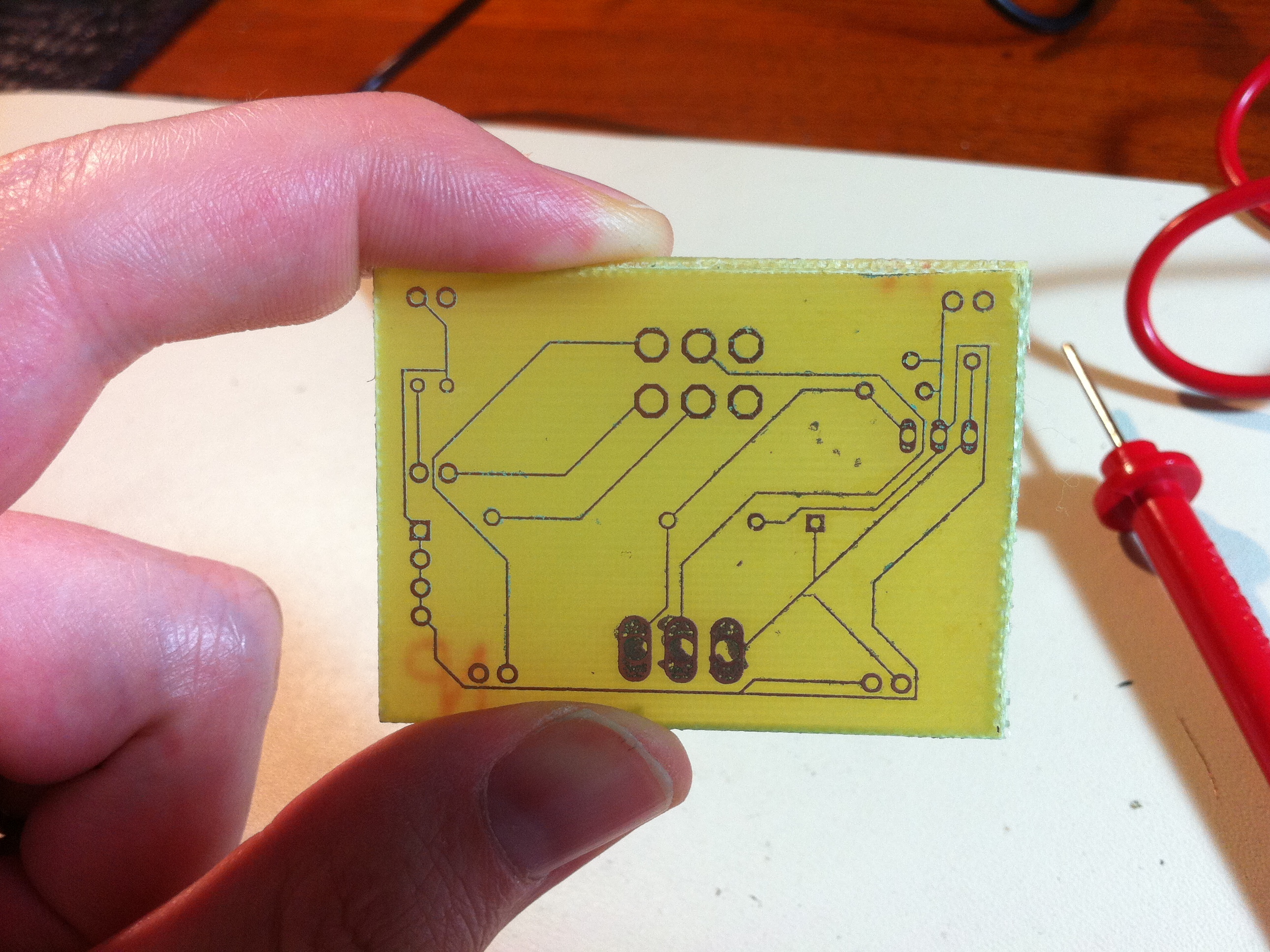
Here’s a sample of the finished product. Those are 0.01″ traces, and they all worked on the first try. This technique is great for small boards and complex layouts. Excuse the mess on the three large pads at the bottom. More on that later.

The first step is to make a board layout. You can’t do much better than Eagle, although the learning curve can be a bit steep. The SparkFun tutorials are a really good place to start. After that, read the manuals that come with the software.

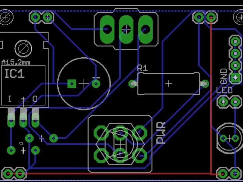
Here’s my board, in Eagle. Note that I tell the autorouter to use 0.01″ traces on a 0.05″ grid, which is contrary to what many tutorials for hobbyists say. This etching technique works well on traces that small, and you can make a much more complex board without resorting to dual layers or lots of jumpers. A layout grid that is double the resolution of the component grid solves a lot of routing problems, in my experience.

I hide all layers in Eagle except the bottom traces, then print it to a PDF. This works great because it’s very high pixel density. That’s critical to getting small traces to work. Many tutorials will tell you to use the Image Export operation, but that generates pixelated images that mess up small traces.

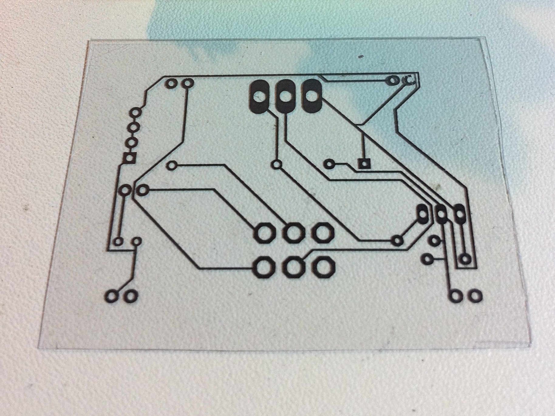
Next, I bring that PDF to FedEx Office (formerly Kinko’s), and print it on regular paper. I then photocopy it to overhead transparency. Kinko’s self-serve printers will not let you print to acetate, but they will let you photocopy onto it. The self-serve printers are a tenth of the cost of going up to the counter, so this two-step method is well worth it.

Why not print it at home? Printers are bulky, ink is ridiculously overpriced, and Kinko’s self-serve is 10 cents a sheet. That’s a lot of PCBs for the cost of owning a printer.

If any part of the printout isn’t totally opaque, use a Sharpie to cover it up. I got a bit sloppy with mine while touching up the three large pads. You can see the result of that in the final product.

Next, I use the photoresist method to transfer the pattern to the board.

This video tutorial from Jameco explains it far better than I could. Plus, Collin Cunningham is hilarious. You only need to watch up to the 4:10 mark. After that, his process is different than what I’m describing.

You’ll need Positive Developer, as well. This is the one and only unpleasant chemical involved. As much as I like Jameco, this stuff from Mouser is 10 times cheaper and works just as well:

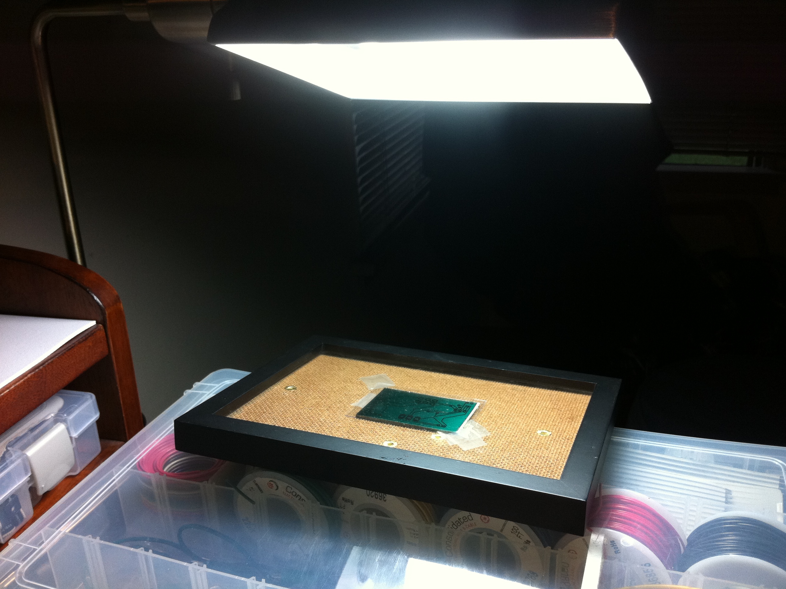
As shown in the video above, I apply the acetate to a presensitized PCB. These are almost as cheap as regular copper boards, and extremely easy to work with. You can expose them with a regular lamp and an old picture frame. It takes only minutes, and because it’s a photographic process, it’s exceptionally precise. Far more so than the song & dance people do with laser printer toner, magazine paper, a clothes iron, and water soaking. I expose the board for twenty minutes with the lamp about as close as I can get it.

Once the board is exposed, sloshing it in a solution of 10 parts warm water and 1 part developer reveals the pattern in all its glory. This takes under a minute.

Now we’re ready for the real work – the etching. For this portion, I can’t give enough thanks to Stephen Hobley and his etching process, laid out in this video.

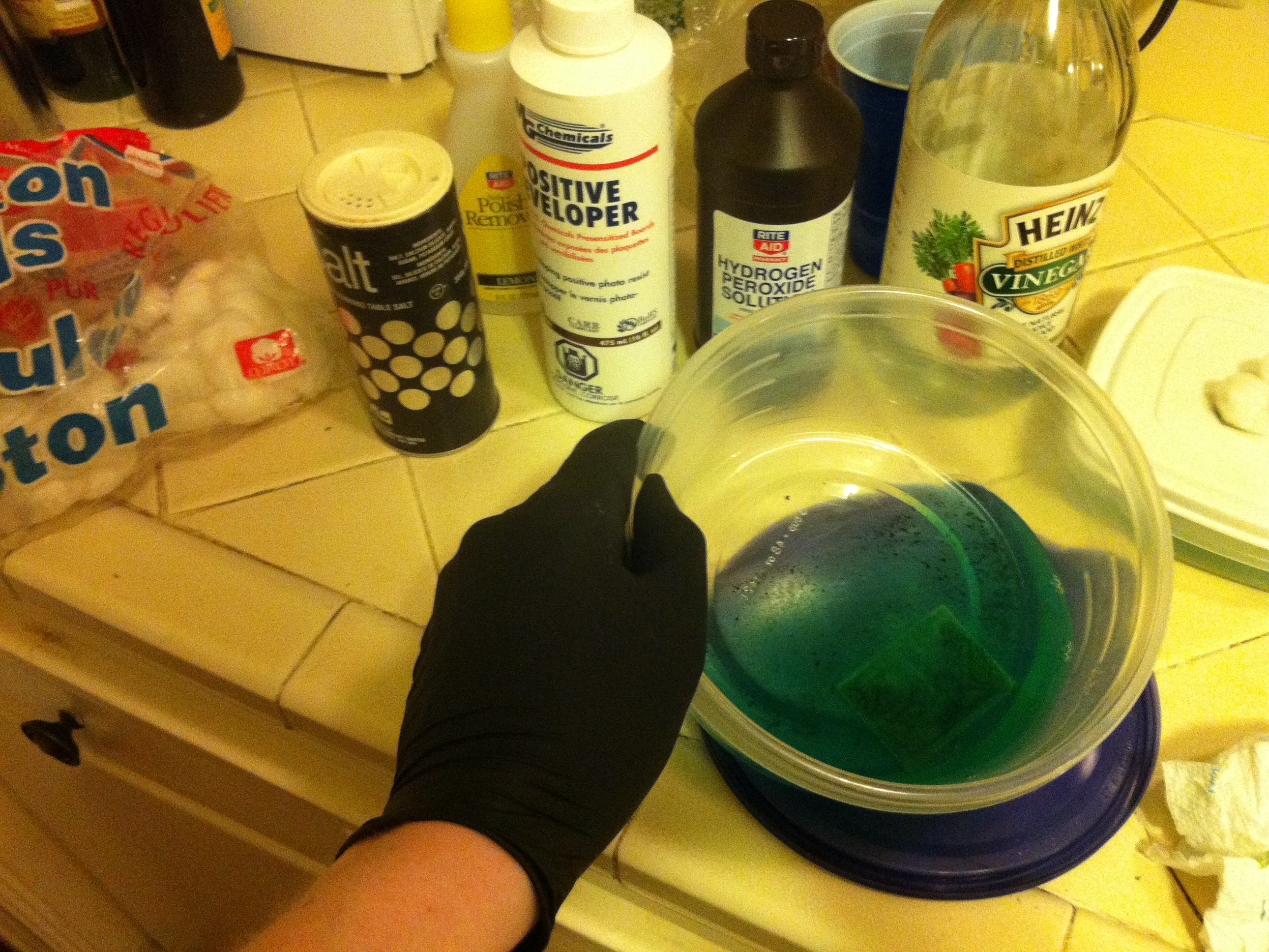
Yes, you can etch a PCB with nothing more than hydrogen peroxide, vinegar, and salt! This mix is so benign you could almost eat it. Please do not eat it. If you do eat it, please do not tell the judge I told you to eat it. Your Honor, if you’re reading this, I explicitly told people not to eat it.

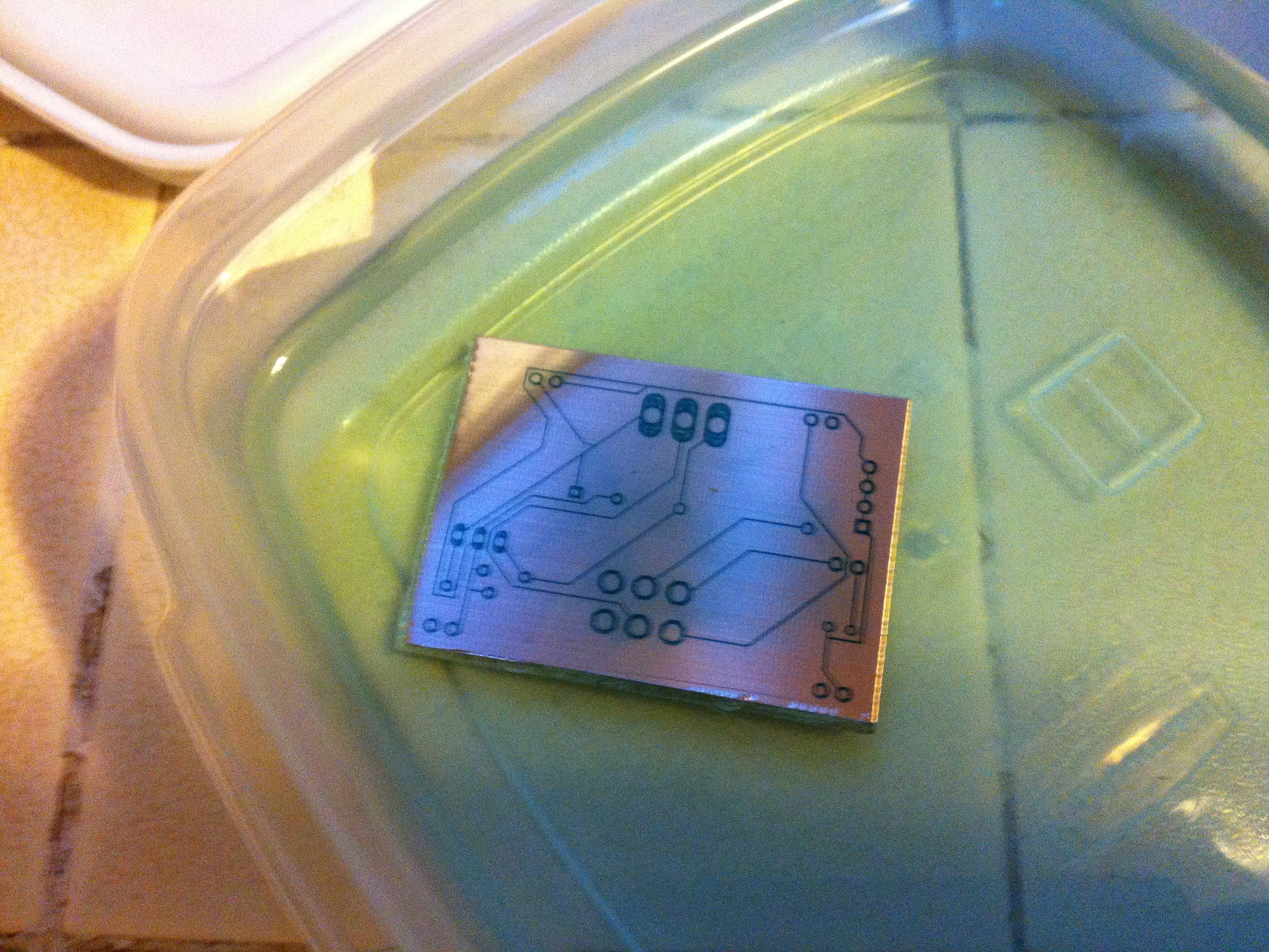
This photo shows my board etching happily in Stephen Hobley’s mixture of 1 part peroxide to 1 part vinegar (which we didn’t eat, right?).

As Stephen explains, dump some salt in there to start, and as needed to keep the bubbles going. Also, open a window, because it smells a bit funky. If this nearly-edible PCB mixing method seems too good to be true, well, there is a catch. It’s slow. The board will require about an hour of soaking, with occasional sloshing and adding salt. Sure, the ferric chloride or muriatic acid methods are faster, but those chemicals are nasty and expensive.

With this method, you can etch a PCB on your kitchen counter, with stuff you probably already have in your cupboard. As slow as this is, it’s sure faster and cheaper than sending away to a PCB house.
Isn’t it purrrty? To drill the normal component lead holes, I use a #69 (.0292″ or 0.75mm) bit in a Dremel. Use larger bits as needed for switch terminals, etc. In my experience, you really don’t need a drill press like everyone says. Just hold the board by the edge with one hand (wear gloves), and drill with the Dremel in the other hand. Wear eye protection and a paper mask! Fiberglass dust is nasty.

Yes, I forgot to add a couple of vias, so there are two under-board jumpers. Oh well, live and learn. So what is this device, you might ask? Well, that’s a story for another time…

For more details and better pictures, be sure to check out this site.

Conclusion

For more details and better pictures, check out this site.