This article appeared in Make: Vol. 90. Subscribe for more maker projects and articles!

We are surrounded by electromagnetic forces, which go largely undetected but are vital to modern technology. Electromagnetic field (EMF) radiation comes from natural phenomena like the planets in our solar system, the heat of a burning fire, the lightning from a storm, and even the beating of a heart. It also emanates from human-made inventions like cellphones, Wi-Fi and other radio signals, lightbulbs, X-rays, microwaves, and much more.

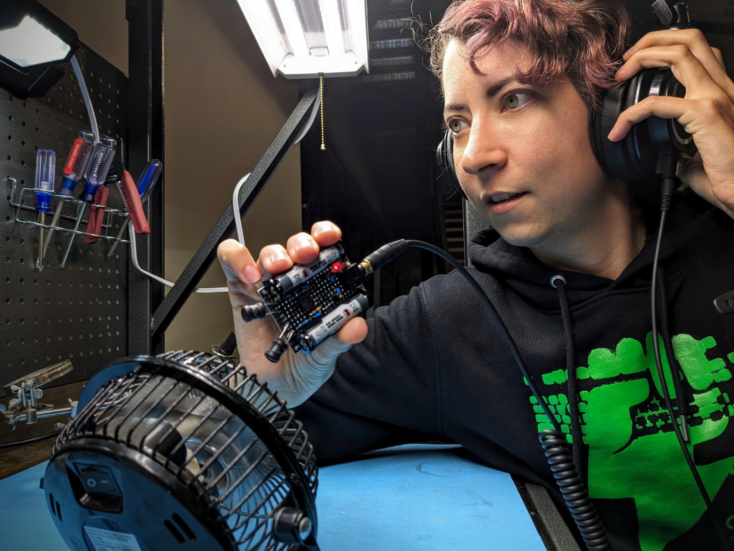
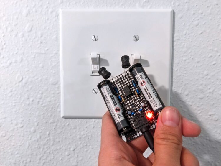
Anything that produces an electric current will emit EMF radiation, creating invisible electronic fields all around us. The EMF Explorer project offers a unique opportunity to tune in and listen, by transforming electromagnetic activity into audible sound. It’s like giving a voice to the silent but constant companions of our electronic era.

YouTube player

The EMF Explorer Project

While this circuit amplifies the majority of EMF signals it picks up, we will only be able to hear those that fall within the frequency range of human hearing, about 20Hz–20kHz. This also happens to be the frequency range that most of our electronic appliances operate within!

Imagine hearing the electronic operations of your cellphone, the rhythmic patterns emitted by Bluetooth headphones, or the electronic harmonies of countless devices whirring along in our lives. This article will guide you through creating your own EMF amplifier at home with minimal parts.

The Project at a Glance

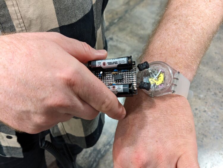
Originally used in an exploratory electronics soldering workshop, this project allows participants to assemble their own EMF Explorer PCB. Inspired by Jonas Gruska’s Elektrosluch circuit and DIY Circuits’ Electromagnetic Field Detector, the circuit was modified to use a smaller battery source, simplified voltage divider, different amplifier and low-pass filter, and optimized to be worn as a wearable PCB badge.

This badge encourages participants to explore the electronics world around them and opens up opportunities for learning about physics, electronic theory, audio applications, and more. It requires only basic electronics know-how and just a handful of components.

Deep Dive Into the Components

  1. Protoboard lets you solder the connections in a durable configuration that should last years.
  2. Inductors are the “sensors” that pick up EMF frequencies and translate them into a measurable signal. Inside are tightly wound coils of wire which, when exposed to an EMF signal, will react and generate a current from the electromagnetic waves in the air.
  3. Op-amp and resistors amplify the inductors’ signal to be loud enough to drive a speaker. We wire up the operational amplifier to create an inverting amplifier, whose gain is determined by the two resistor values connected to the op-amp.
  4. AAA batteries and holders provide the necessary dual-voltage supply for the op-amp.
  5. Capacitors sculpt the signal, shaping and filtering the electromagnetic waveforms. The .01nF capacitors help to stabilize the output of the op-amp from the massive gains we are pulling from it. Optional 10µF capacitors act as a low pass filter, cutting out some of the high frequencies for easier listening. Experiment and decide which sounds you prefer.

What will the next generation of Make: look like? We’re inviting you to shape the future by investing in Make:. By becoming an investor, you help decide what’s next. The future of Make: is in your hands. Learn More.

Project Steps

1. Place the Batteries

Before you begin soldering, make sure you’re working on a heat-resistant surface and have ventilation for the solder fumes.

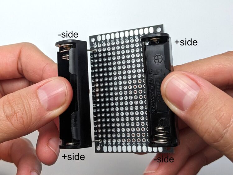
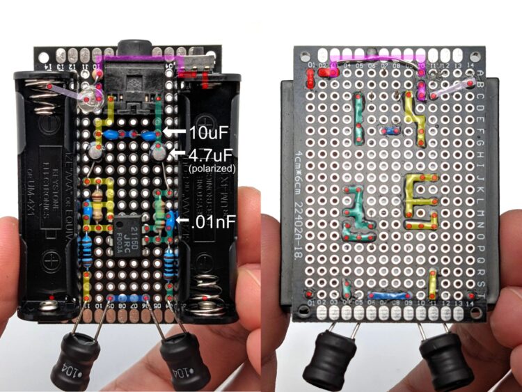
The battery holders take up a bit of space on the board; add those first so you’ll know how much room you have for the rest of the circuit. Place them on the outermost sides, and leave an open row at one end so that they take up the least amount of space possible. Make sure the position and polarity of the batteries match what you see in the photo.

2. Add the power control

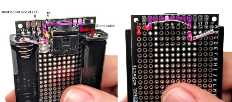
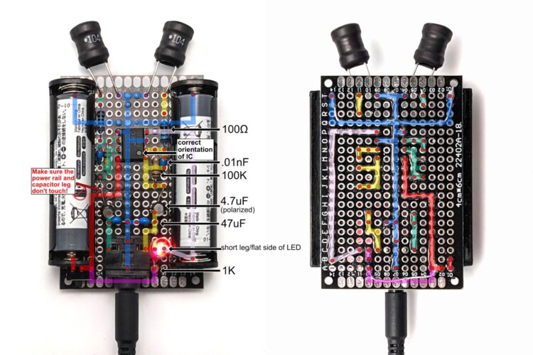
Add the LED, LED resistor (1K), and switch, and place the output jack, as shown. You won’t solder the jack quite yet, but snap it into place now to ensure everything will fit. The red dots indicate the holes that each component is placed through, and the color stripes indicate the connections on the underside of the board.

When soldering together components, use the leftover length of the leads to help make the necessary connections. The short leg/flat side of the LED will connect to the negative (–) battery terminal, and the long leg will connect to one side of the resistor. Connect other leg of the resistor to the switch, being sure it doesn’t touch the jack. Notice how I soldered the LED leg to one of the outer pads to help ensure that it never touches the jack.

Once everything in that section is soldered up, cut the remainder of the leads off.

3. Amplify Your Signal

In order to hear the signals being picked up by the inductors, we need to amplify them up to human hearing levels. The resistors determine how much the op-amp amplifies the incoming signals from the inductors.

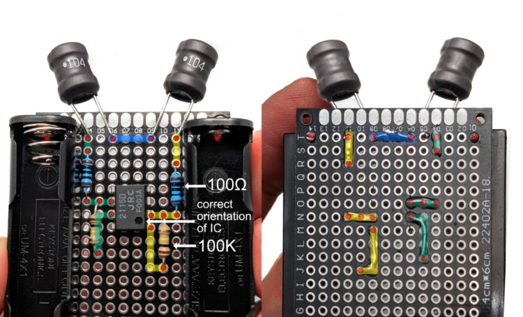
Add the inductors, the four remaining resistors, and the op-amp IC as shown. Make sure that the black dot on top of the IC matches the orientation shown, and that the resistors are connecting to the correct legs of the IC. Solder the connections together, again using the leads to help make the connections, then trim off the excess leads.

4. Add the Caps

Now you’ll add all the capacitors and connect them into the audio jack outputs. For this part, you’re going to run the positive leg of the 4.7µF capacitors on the top of the board, toward the resistors. Notice that the 4.7uF caps are polarized, meaning the orientation of the white stripe needs to match what you see here. Place a piece of electrical tape or paper underneath the topside leg to make sure it doesn’t touch any other pads on the board, as you will later be running power across the underside.

Make sure everything is laid out correctly before soldering in place.

5. Lay out the Power!

Finally, add the power distribution across the board. Connect the remaining four legs of the IC, the center trace that connects the inductors, the 10µF caps, and the ground pin of the audio jack to the appropriate power rails, as shown. For connections along the longer traces, you may want to use some of the excess leads you trimmed from the other parts.

6. Inspect and Test

Take a moment to carefully review your board and ensure that everything is connected as it should be. Trim off any excess leads.

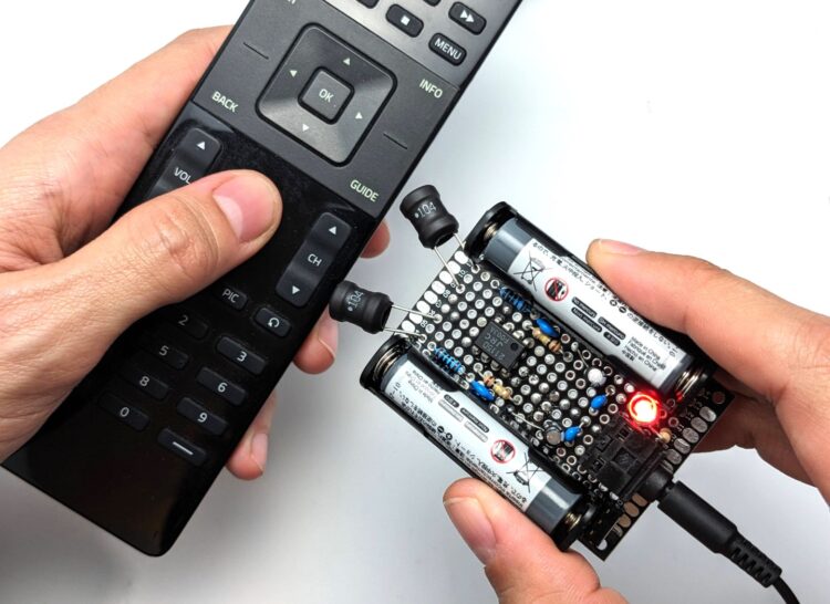
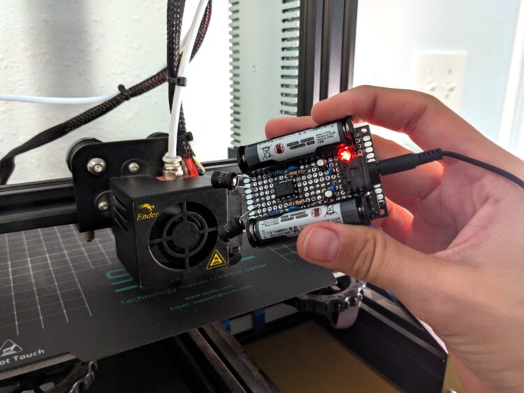
Now you can add the batteries and plug in your headphones! Bring your EMF sensor close to a powered electronic device like a computer, phone, wireless headphones, etc. You should hear a buzzing sound as you get closer to the power source.


The Adventure Begins

With your EMF amplifier in hand, it’s time to go exploring. Venture out to discover the hidden electronic symphonies around you.

Each electronic device offers a unique acoustic signature, from the bleeps of Bluetooth headphones to the varied sounds of different gadgets. How do a computer’s sounds differ from that of a lightbulb? Can you distinguish a cellphone’s different chatters coming from its various components? See how many types of sounds you can discover.

You can also experiment with different component values to adjust the gain, low pass filter, inductor size, and more. This op amp uses the same footprint as many other common two channel op amps, so you should be able to swap that out as well if you’d like, but be aware of the pinout and min/max voltage limits of the op amp you’re choosing.

Conclusion

A Portal to the Invisible

The EMF Explorer project is a gateway to building a deeper understanding of our surroundings and the complex electronic ecosystem that supports our modern life. As a continuation of this project, I’ve designed this circuit into a wearable art PCB (printed circuit board) using KiCad, an open source PCB design software. I did this by hacking the technical layers that make a PCB and repurposing them as visual art layers. Like painting on a canvas, the elements of a circuit board can be used for visual imagery.

To do this, I created vector images for each PCB element and then assigned them to the appropriate layers in KiCad, which includes the copper layers, solder mask layers, and silkscreen layers, all of which can be used in nontraditional ways to create a unique color palette.

To learn more about the PCB design process and the EMF badge itself, check out my website, or you can buy the kit on the Maker Shed!

All photos by Darcy Neal. This article appeared in Make: Vol. 90. Subscribe for more maker projects and articles!