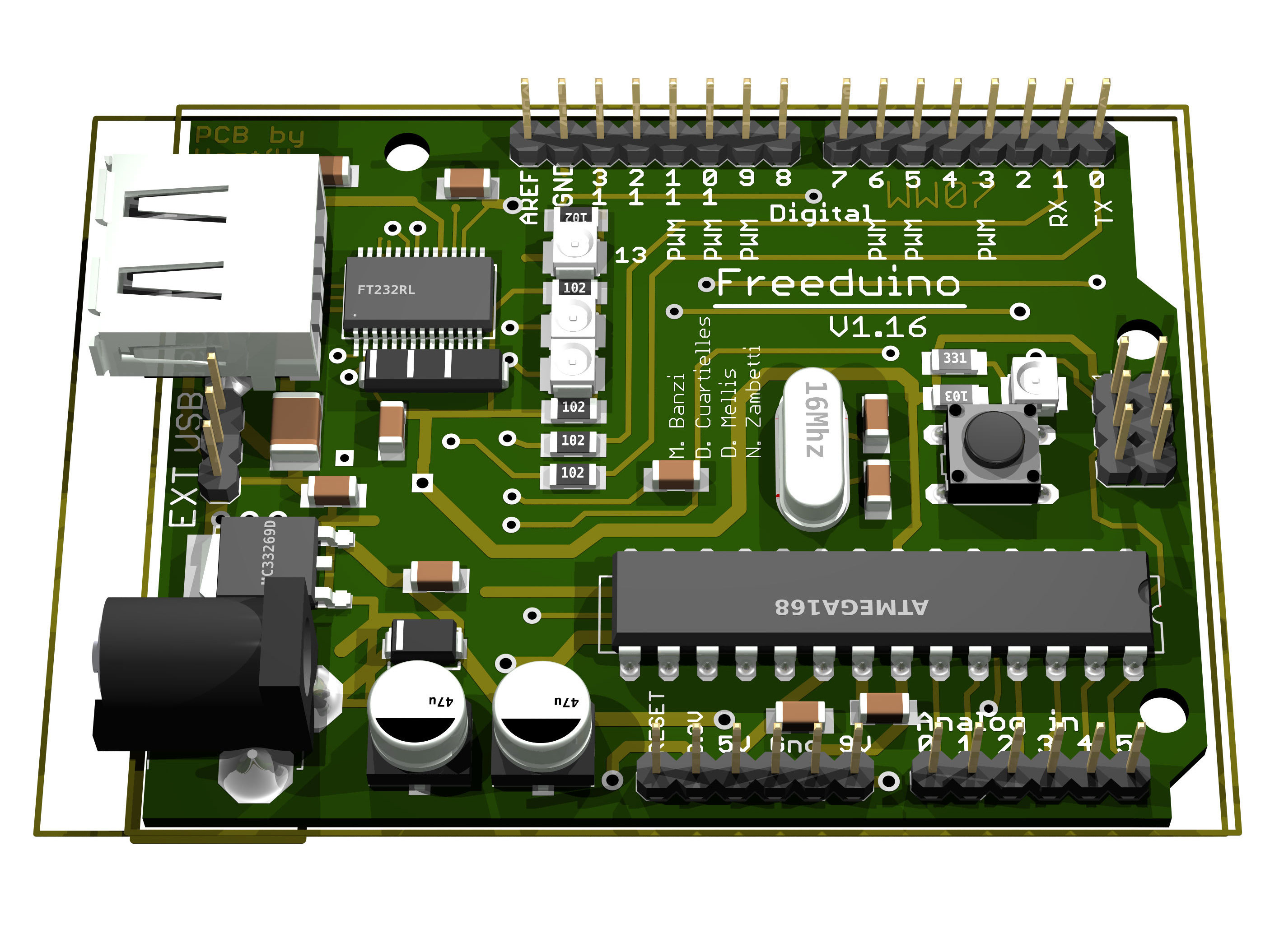
This project will cover the basic use of CadSoft’s Eagle freeware. We will be exporting from Eagle to the DXF file format which is readable using Adobe Illustrator. From there, we will take separate exports to show the overall sequence events involved in desiging the board. But first we start with the board layout.

What will the next generation of Make: look like? We’re inviting you to shape the future by investing in Make:. By becoming an investor, you help decide what’s next. The future of Make: is in your hands. Learn More.

Project Steps

Components

The first step in designing a circuit board is laying out the components. This process Can be challenging because there is no one correct layout of a given circuit.

In general you want to place connectors near the edges of the board for easy access later.

Depending on how the board is going to be installed also determines where you want to place any LEDs or other indicators. They need to be installed so that you can see them.

These images show the outline of the board with the components placed and the board size defined.

Components Cont.

This is the schematic modified to only show the components. These are the parts that need to be placed onto the board

Traces

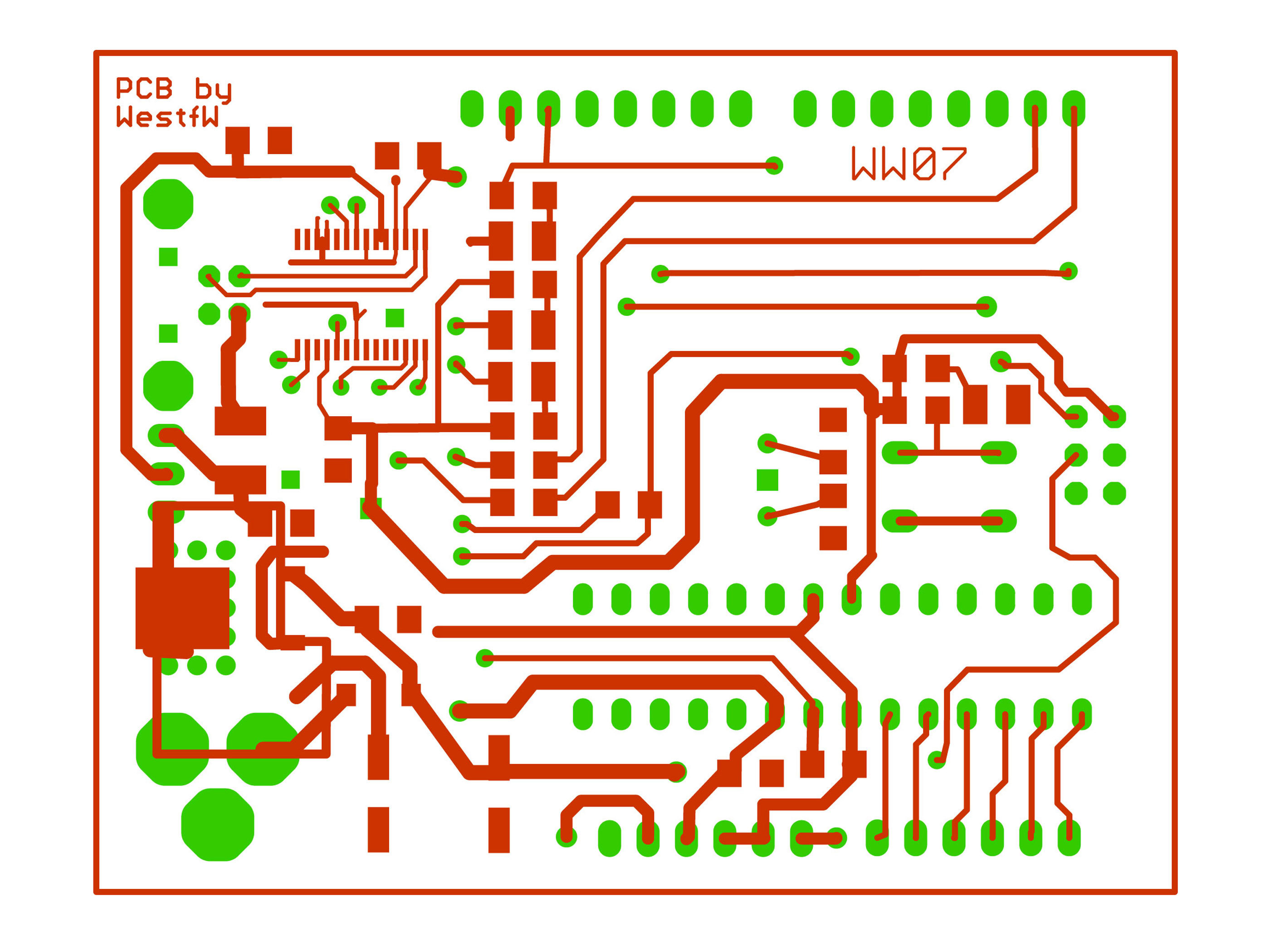
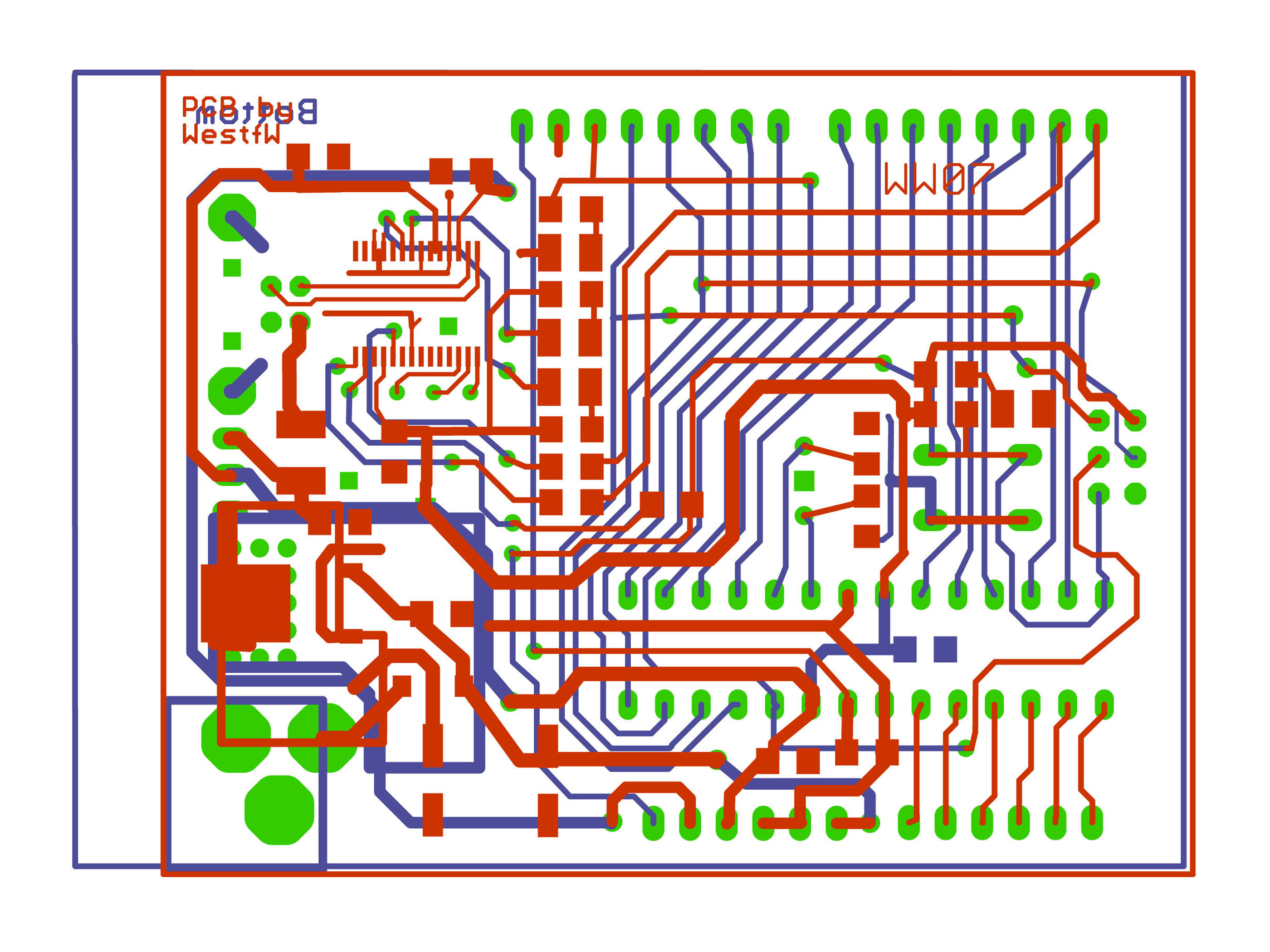
The next step is laying out all of the traces between the components.

The traces are the wires that connect all of the parts of the circuit together.

This board is a two layer board. This means there is a board made out of fiberglass sandwiched between two layers of copper.

The red traces are on the top side of the board.

The blue traces are on the bottom side of the board.

Traces are routed between the top and bottom of the board by Vias

A Multiple layer board allows for much greater flexibility in designing a board. With one layer, none of the traces have the ability to cross another trace. Adding a second trace lets traces cross, which makes more complicated designs possible

Traces Cont.

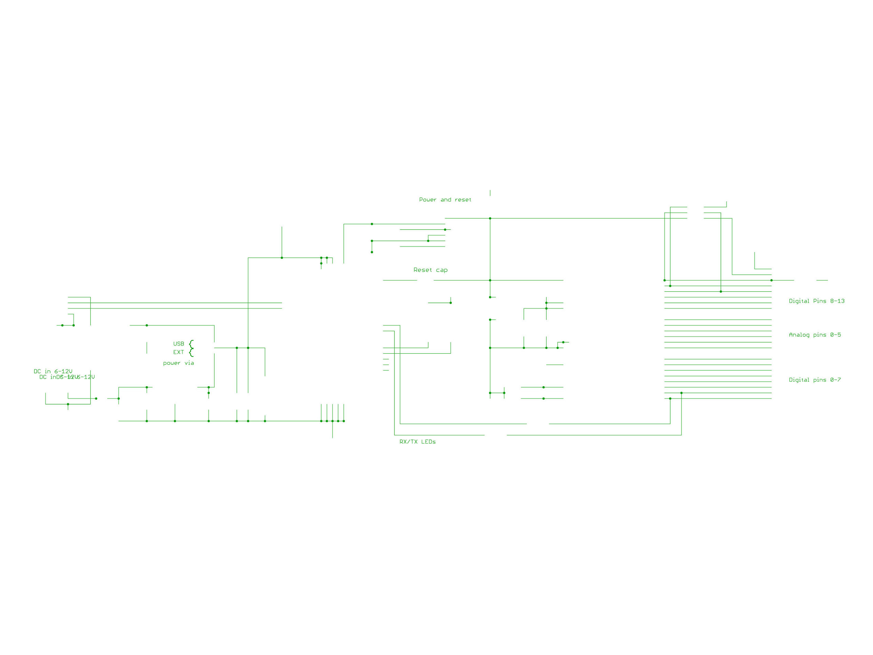
This is the schematic modified so it only shows the nets. These connections are what are translated into the traces on the finished board.

Soldermask

Next, you add all of the production information for solder masking and reflow. Everything from this point on in the guide is optional, and depends on where you are getting your board fabricated, and what options you choose.

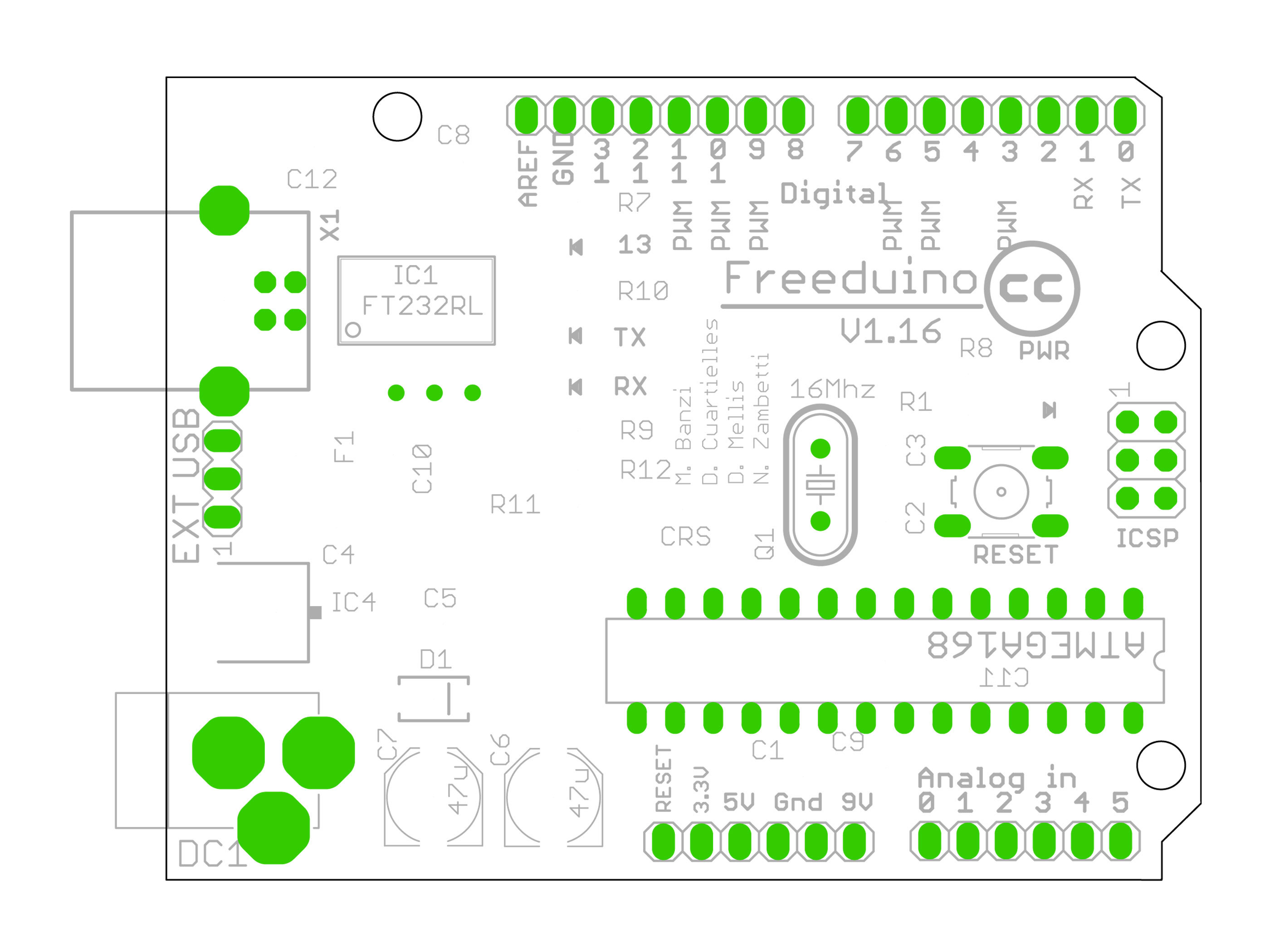
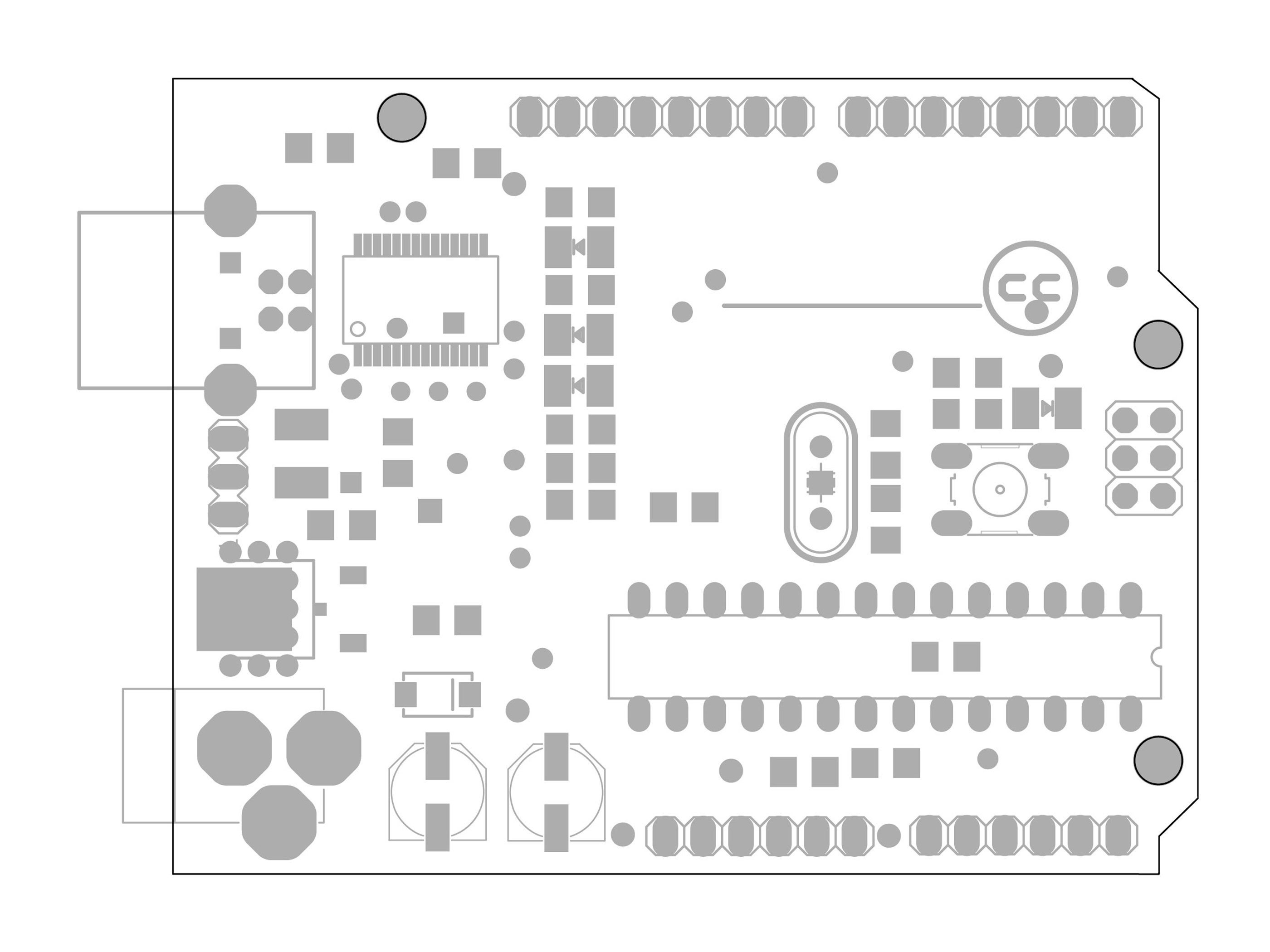
The first picture is the soldermask layer. Any places grey on this image will have no soldermask placed onto them.

Soldermask is a layer of material placed on the board that solder doesn’t stick to.

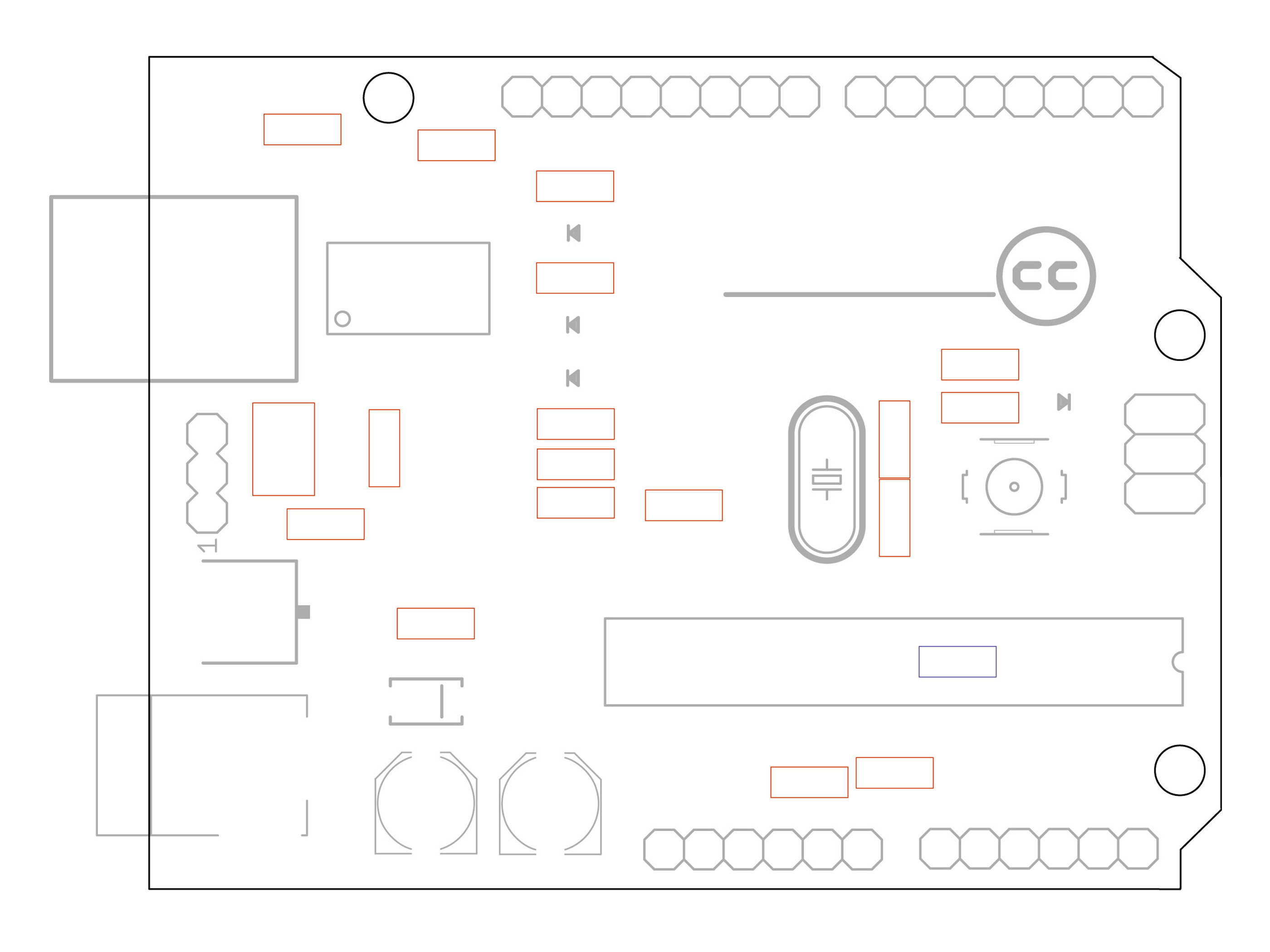
The picture is the solder paste layer. Solder paste is small particles of solder mixed into a paste. It is placed onto the pads on the board, followed by the components. The entire board is heated and the solder melts, soldering the surface mount components down.

The third picture is the glue layer. Small dabs of glue are placed onto the board in order to hold parts down during assembly before they are soldered into place.

Keepouts

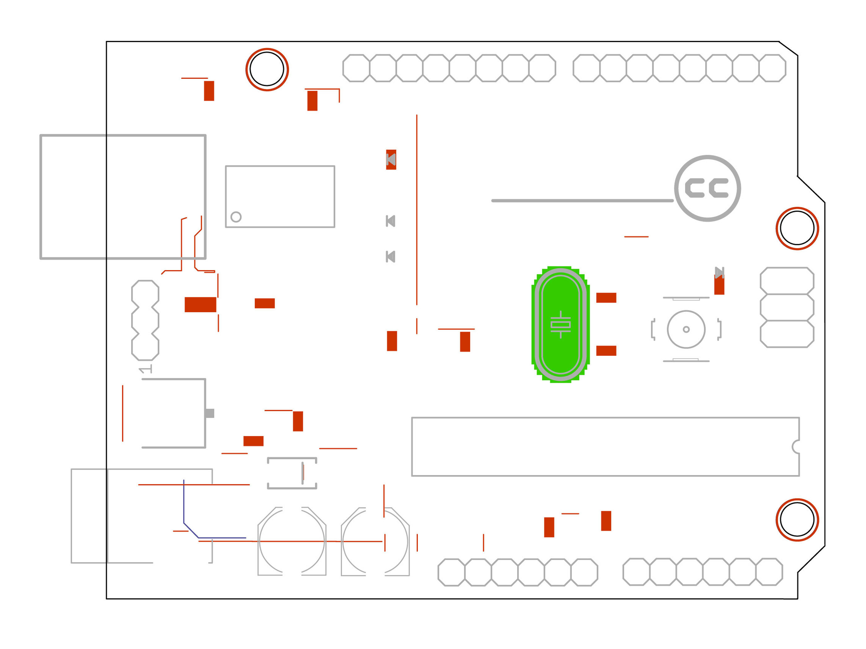
The first picture here is the component keepout layer. When designing the board, you can designate areas where you’re not allowed to place components due to physical size restraints and constrictions.

An example of this would be keeping a component out of the area where a heat sink would go.

The second picture is similar, but for traces. Wires are not allowed to travel through the designated areas.

The green area in the second picture is the via keepout area.

Most of the keepout zones are placed in order to use automatic board design software such as autorouting tools. These tools will automatically place all of the traces on the board, but are not smart enough to make proper engineering choices.

Silkscreen

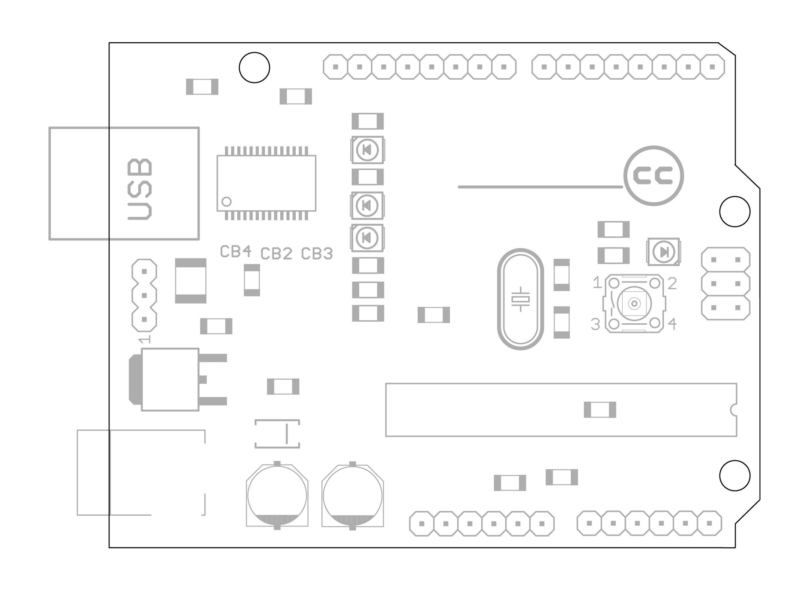
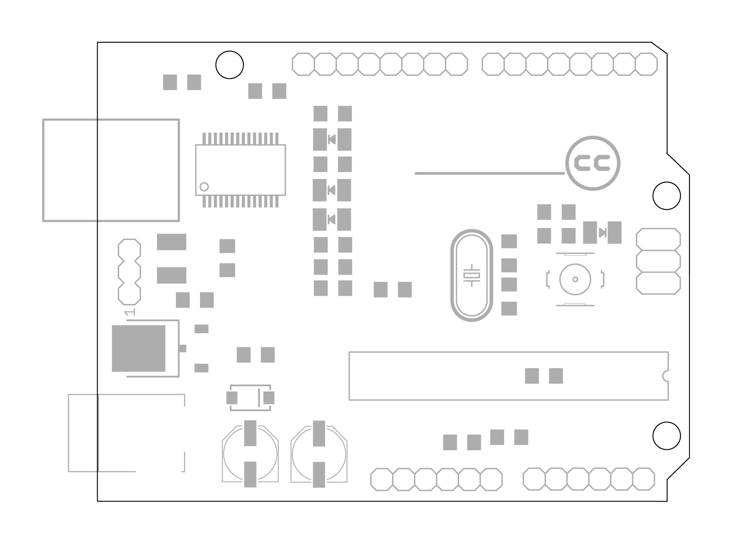
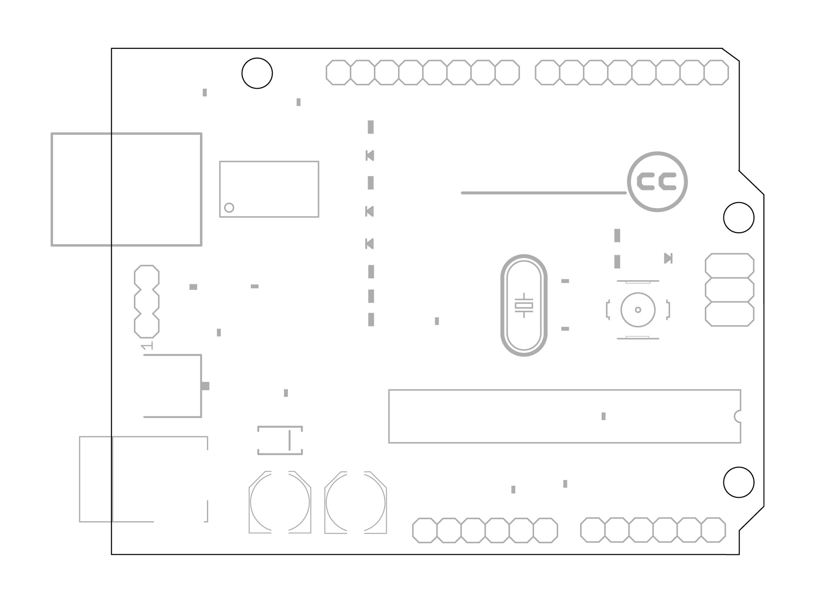
Finally we have the silkscreen layer. This is a layer of printing that is printed onto the board to help with assembly, as well as add a professional finished look to the final product.

The availability and color of the silkscreen layer depends on where you get the board manufactured.