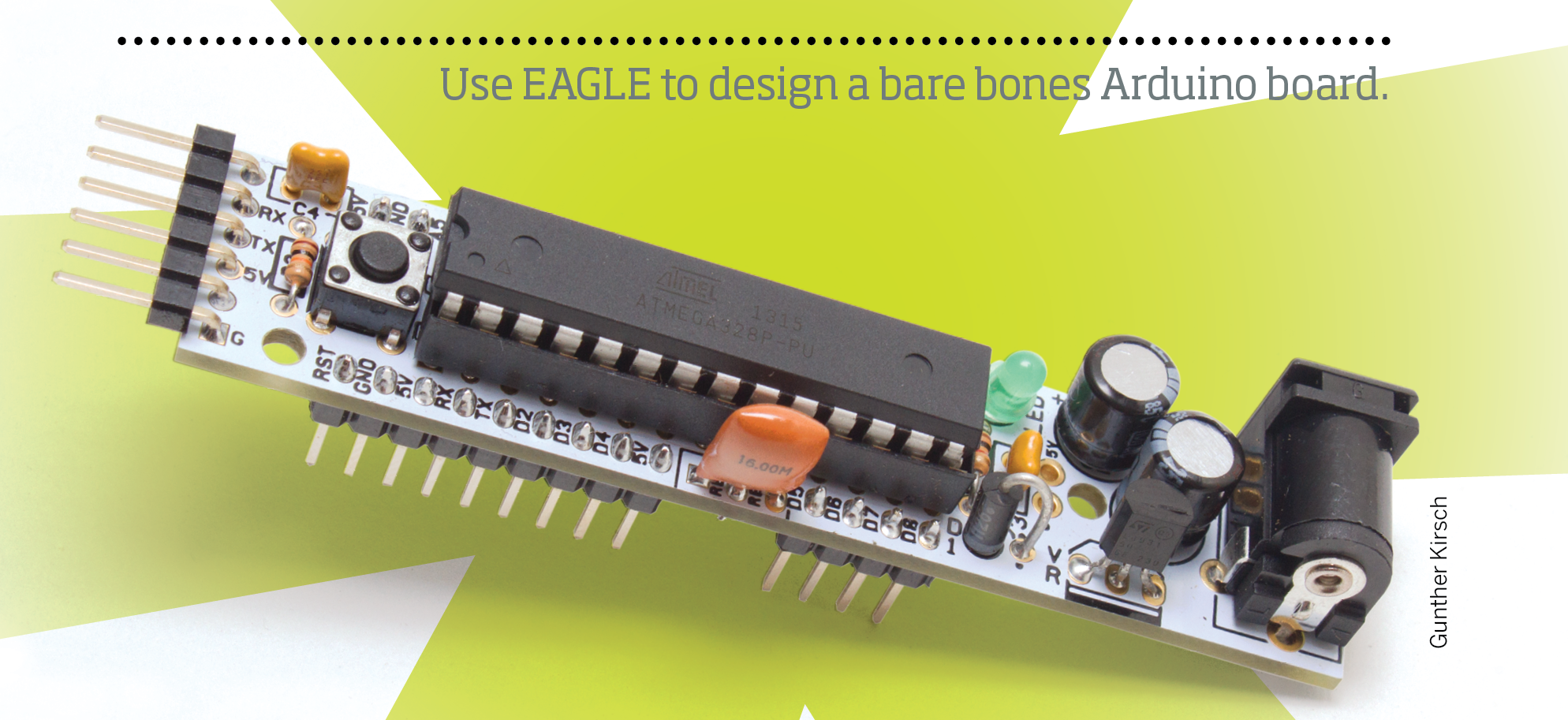
The files you send to the PCB manufacturer are in the Gerber file format, a standard CAM file format for PCBs. Gerber files are created using the CAM processor under the File menu. You’ll also need to create a drill CAM file in the Excellon format. You’ll need (at least) the following Gerber files, which are specified as either “Component-side” (top) and “Copper-side” (bottom):
| Layer |
File Extension |
| Component-side copper |
.cmp |
| Excellon Drill CAM file |
.drd |
| Component-side silkscreen |
.plc |
| Solder-side copper |
.sol |
| Component-side stop mask |
.stc |
| Solder-side Stop mask |
.sts |
Note: Many services allow silkscreen on the top and the bottom of the board. To add a silkscreen design to the bottom you’ll have to add a new Gerber file to the CAM job with a “pls” extension.
3.1. To create the CAM files, open the CAM Processor from the File menu. Note that this tool is context-sensitive whether you’re in the schematic or board view, so make sure you’re in the board view. Open the excellon.cam job to create the drill files (with extensions .dri and .drd). You only need the .drd file; the .dri is just metadata.

3.2. Next generate the Gerber files by opening the gerb274x.cam job. The only section you should need to double check at this point is the Silkscreen tab; if you’ve added a bitmap layer (or don’t want a layer on the silkscreen), make sure to assign the correct layers on that tab.

3.3. To preview your files you’ll need a Gerber viewer tool. Gerbv is a good open source option if you’re on a Unix-based system, or you can use ViewMate on Windows. If you’re on a Mac Gerbv is a little tricky to get up and running, so you should try to use a package manager like MacPorts to install it. The easiest solution to previewing Gerber files is to use the free online tool from Circuit People.

3.4. Import the layers into your gerber viewer (Gerbv is shown below). I usually re-organize them from top to bottom to make it easier to proof:
- .drd
- .plc
- .stc
- .cmp
- .sts
- .sol

Turn each layer on and off and inspect, if you tweak the layout, rerun the CAM processor.
Note: If you move a part, remember to run the Excellon drill job as well. Otherwise your holes won’t match up with your pads!
3.5. Bundle them up and send them out. As great service for small runs is OSHPark, which grew out of the DorkbotPDX service and merged with Sparkfun’s BatchPCB service. The interface is well designed and service is quick and consistent, with a free shipping option. Your board will be bundled with dozens of others and will come back with a distinctive purple soldermask. If you need more than a dozen boards it is more economical to go with another service. There are many competitive options (and more popping up in the US); I’ve had good luck with the affordable PCBCart service.
Note: OSHPark and some other PCB services require an additional Gerber file that is not created by the default gerb274x CAM job. You’ll need to add a “Board Outline” section that represents the board outline. With the job open in the CAM Processor, select “Add”, then select just the Dimension layer. Change the file name to “%N.gko” and you’re good to go.
If you have any suggestions to add, or ways we can improve this article, please post in the comments below. Happy routing!