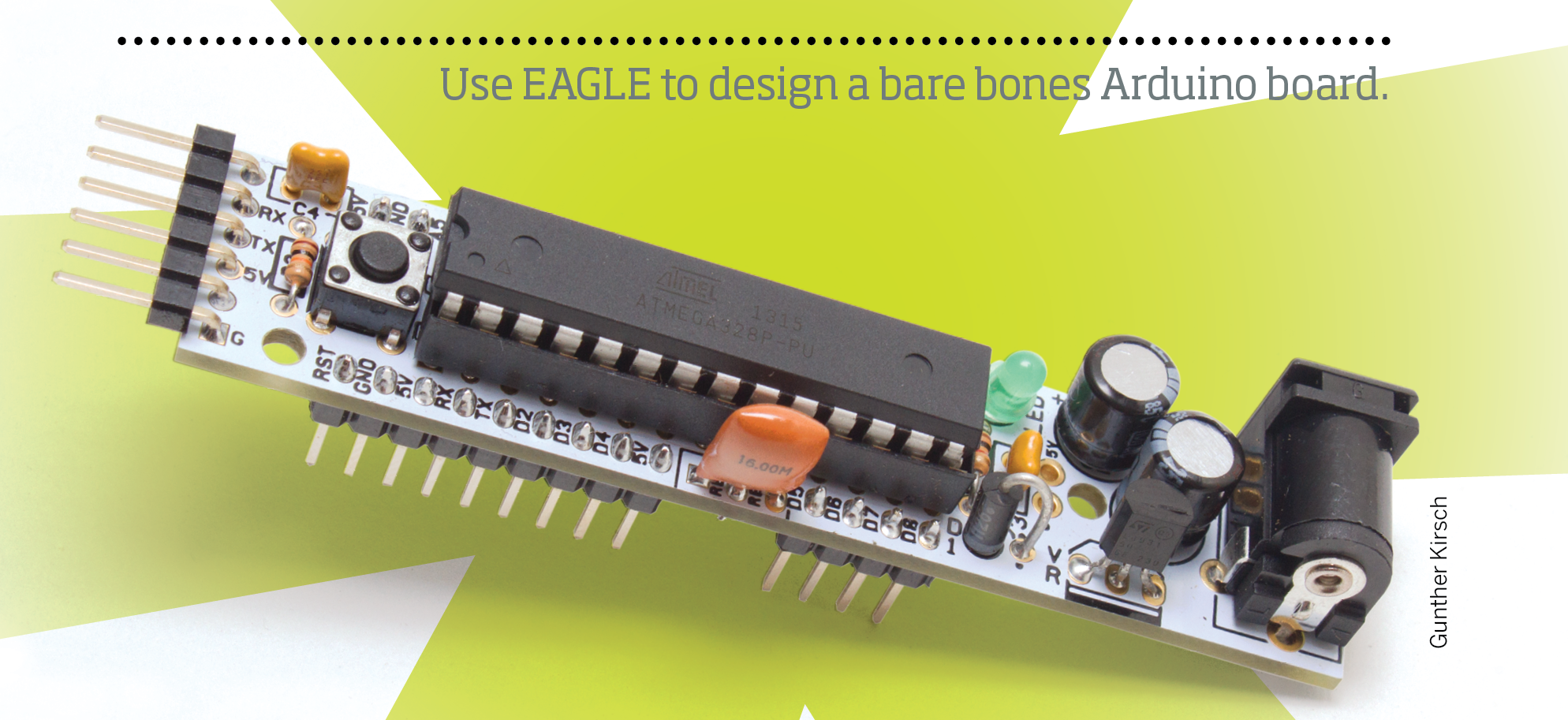
The Really Bare Bones Board

This series of 3 tutorials introduces the use of CadSoft’s popular free-as-in-beer EAGLE PCB design suite. We’re learning the ropes by stepping through the design process for a basic Arduino-type AVR microcontroller development board, specifically the Really Bare Bones Board design by Paul Badger of Modern Device.  In Part 1, we showed you how to lay out the schematic and validate it with EAGLE’s built-in Electrical Rule Check. Here we’ll show you how to establish the physical shape of the board and the actual copper pathways that make up the real circuit.

Once your schematic has passed the ERC, you’re ready to start routing the board. EAGLE has a tool that will automatically route all the traces on the board following rules you specify in Design Rule Check (DRC). I won’t get into the argument over autorouters vs. hand routing, except to say that it is a good idea to at least try your hand at manual routing to get the hang of it. That’s what we’ll do here.

Project Steps

1. Getting started.

When you’re ready, select File → Switch To Board and you’ll be asked if you want to create a new board from the current schematic using Layout Editor. From now on you’ll always want to have both schematic and board windows open whenever you’re doing work. EAGLE will keep the two in sync, but only if they’re both open.

BoardLayout1

When you first open Layout Editor you’ll see a jumble of parts to the left and a rectangular work area to the right. The free version of EAGLE is limited to 4″ x 3.2″, and you’ll get a warning message if you try to place a part outside this boundary.

The black lines defining the boundary of the board layout are drawn on the Dimension layer. Because we’re working from an existing design, the first thing to do is to draw the actual boundaries of the board; the RBBB is 3.0″ wide by 0.6″ tall. This is pretty much the smallest footprint in which you can fit all of the parts while still leaving room for some labels.

Choose the Line tool and select the Dimension layer from the top toolbar. Draw the board outline as shown above. This defines the routed edge of the board; you can draw complicated shapes as long as you keep in mind the limitations of a router bit.

NOTE: As with the schematic it is very important to keep a consistent grid. The general rule of thumb is to keep the grid as coarse as you can until you need to make it finer. When routing traces you’ll need to set the grid to 0.025″ (25 mils). Do that now under View → Grid.

2. The power circuit.

Now move some parts onto the board. Grab a part by clicking its crosshair, which is the part’s “origin.” These origins are on their own layers (tOrigins and bOrigins); if these layers aren’t visible, you won’t be able to grab the part to move it.

BoardLayout2

2.1. As before, start with the power circuit. Move the power jack, the regulator, the diode, the two power capacitors, and the auxiliary input header JP1 into place as shown. The exact placement doesn’t matter too much, as long as you keep them in the rightmost 0.9″ (or so) of the board outline.

You’ll notice the yellow “airwires” (unrouted connections) that run between the various parts, which correspond to the way the parts are connected in the schematic. As you move the parts the airwires will follow; keep an eye on how they’re connected when you’re placing them and use the Rotate tool to turn parts around to make connected points closer and easier to route. Here, for example, the diode could be rotated to make a shorter connection to the input 47μf capacitor.

BoardLayout3

2.2. It’s generally a good idea to place all the components first, and route them after, but in this case we can route as we go. Select the Route Manually tool and use the default trace width of 16 mils. Select the bottom layer, then click on the topmost pad of the power jack; this is the Ground pad. You’ll see all the other nearby ground pads become highlighted.

Route traces between all of the Ground pads as shown. It’s good practice to avoid sharp corners, the behavior of which you can change in the Wire Bend section of the toolbar.

BoardLayout4

2.3. Next, route traces to connect the power pads as shown.

BoardLayout5

2.4. Move the 0.1μf capacitor (C3), the 1K resistor, and the “pilot light” LED onto the board. Use the Rotate tool to position them correctly, then route the traces.

3. The GPIO pins.

BoardLayout7

3.1. Place the ATmega microcontroller, the 3 GPIO headers (JP2, JP3, JP4) and the resonator as shown here.

NOTES:

  1. Place the microcontroller with the semicircle notch facing left. This indicates the side of the chip with pin 1.
  2. Make sure that the headers are exactly 0.5″ apart (on center) on the y axis. That way they’ll fit perfectly across the “trench” in the center of a standard breadboard.
  3. Make sure that the headers are oriented correctly. Depending on how you connected them in the schematic, you may need to use the Rotate tool. JP2 should have +5V as the leftmost pin, JP3 should have RESET on the left, and JP4 should have D4 on the left.
  4. The resonator goes right next to ATmega pins 8, 9 and 10. The high frequency signal lines between the resonator and the chip should be as short as possible, and other signals should be kept away from the area around and beneath the resonator, to prevent unwanted Radio Frequency (RF) interference.

BoardLayout8

3.2. Start routing with the signal and power lines on the top layer of the board. Another good rule of thumb is to keep your ground connections all on the bottom layer if possible. That way they can all be connected together in the largest possible ground plane.

BoardLayout9

3.3. Connect all the ground pads on the bottom layer.

4. The reset switch and serial header.

At this point you should only have 4 parts left: the reset switch, the 10K reset pull-up resistor, the reset capacitor, and the 1×6 serial header.

BoardLayout10

4.1. Move the remaining parts onto the board…

BoardLayout11

4.2. …and route the traces on the bottom.

boardlayout12

4.3. Route the 3 signals shown above on the top layer.

5. Adding the via.

Now only 2 unrouted signals should remain as yellow “airwires” in your window. The +5V signal can be easily routed on the top side to other traces on the board. The reset signal—connected to the left top pad of the reset switch—will need to be routed between the top and bottom using a via, which is a plated hole that connects traces between two sides and/or layers of a PCB.

boardlayout13

5.1. To make a via, start a new trace by clicking on the first pad at the reset switch. Route a path, as shown, until you get to the open area just before your trace will hit other traces on the bottom layer.

boardlayout14

5.2. With the Routing tool still active, go to the toolbar and select the top layer. Finish the route to the connecting pad on the top layer.

boardlayout15

NOTE: When you finish the path you’ll see the small plated via pad appear as shown above.

Via

5.3. You can use the Change (wrench) tool to change many attributes of a part after it has been placed or drawn. Change the shape of your via from square to round, by first selecting Shape → Round from the pulldown menu, then clicking on the via.

boardlayout16

5.4. Route the last trace as shown.

6. The ground plane.

As with many of the tools in EAGLE, the workflow for drawing a ground plane is a bit counterintuitive if you’ve used other tools, but is pretty simple once you’ve done it a couple of times.

6.1. First select the Polygon tool, then draw a polygon box around the perimeter of the board (it doesn’t matter how close you are to the edge).

6.2 Now select the Name tool and click on the polygon. You’ll get a dialog box as shown. Change the name of the polygon to GND and it will be automatically connected to all of the other GND pads and traces. When you hit the Ratsnest button you’ll see the polygon fill all of the empty space on the bottom with a ground plane connected to GND.

7. The Design Rule Check

DRC

The Design Rule Check is the board layout equivalent of the ERC; select it from the Tools menu when you’re done with the board. That will bring up a tabbed panel where you can set a number of design constraints to test your board against.

For example, if your PCB fabricator tells you that traces should be no closer than 6mils, you can set that in the DRC and see if any traces come too close. Or if you’re making a beginner’s kit and want your pads to all be a little bit larger, you can set this under the Restring tab. The default values are all pretty good though, so you don’t have to change anything here and it should still turn out fine.

When you run the rule check you’ll get a window with errors and warnings. In some cases you may choose to ignore or clear warnings if you know what you’re doing, but unfixed errors will almost certainly result in a non-working board.

Going Further

BoardLayout18

That’s all there is to routing; the only steps left are to create the silkscreen layer and the Gerber and drill files to be sent to the PCB house. Read all about how to do that, right now, by clicking through to part 3.