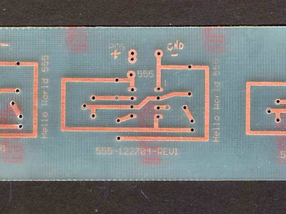
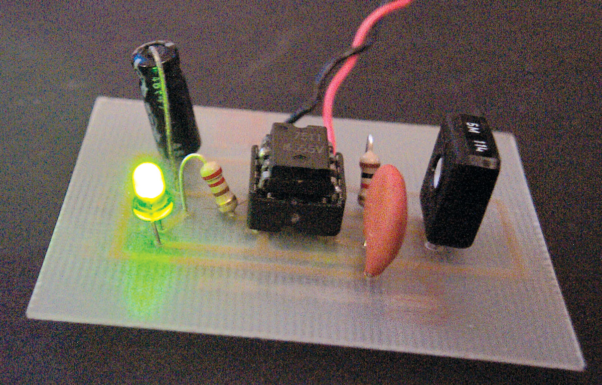
Making your own printed circuit board (PCB) might seem a daunting task, but once you master the steps, it’s easy to attain professional-looking results.
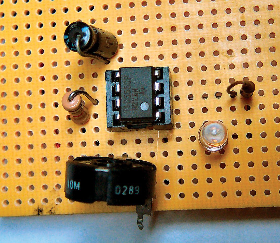
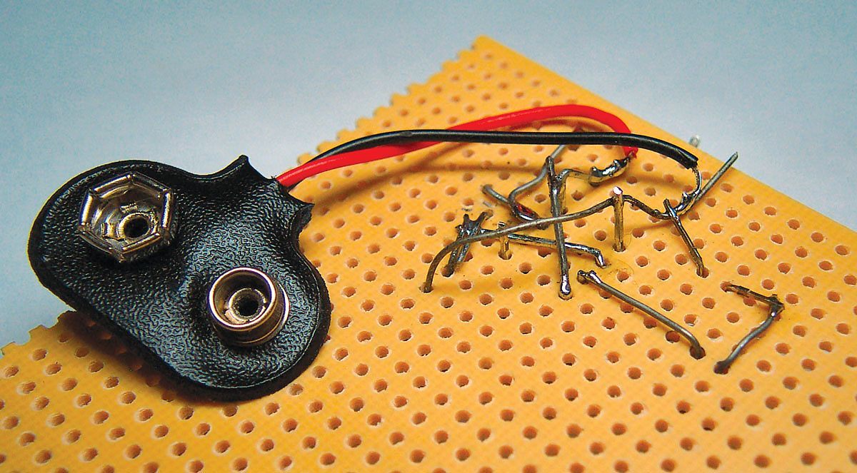
Printed circuit boards, which connect chips and other components, are what make almost all modern electronic devices possible. PCBs are made from sheets of fiberglass clad with copper, usually in multiple layers. Cut a computer motherboard in two, for instance, and you’ll often see five or more differently patterned layers. Making boards at home is relatively easy, but limited to one- or two-layer designs. Here’s how to create a one-layer board for a blinking LED circuit. For PCBs, this exercise is the equivalent of a beginner’s “Hello World” program in software.
PCB: Make vs. Buy
You can order custom PCBs through design houses, but they are expensive — and the per-unit cost is especially high for small batches. Also, when you change the design, a shop will typically take several days to turn it around. Since it’s normal for a board to go through several revisions, this adds up to a significant delay.
Advantage of PCBs
Circuitry built on custom boards is sturdier, more stable, and more compact than the same electronics strung together by hand. And since it takes less time to assemble, PCBs are also better for making multiples. They’re cheap and easy to prototype, and you can find a variety of templates and projects online.
TIP: PCB design houses are well worth the price if you have a finished layout. But if your project is relatively simple, or the design is still evolving, then making your own PCB is the way to go.
Process Overview
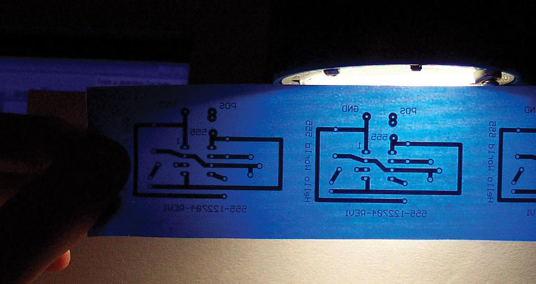
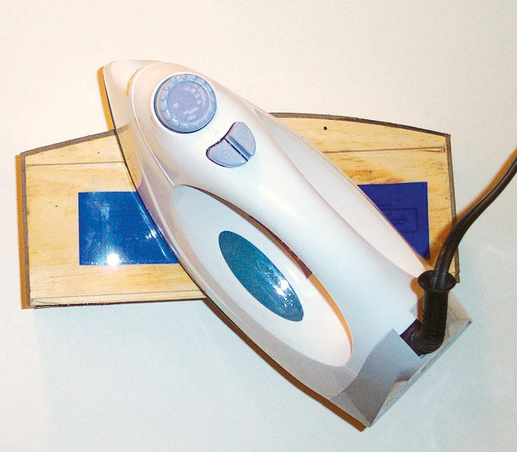
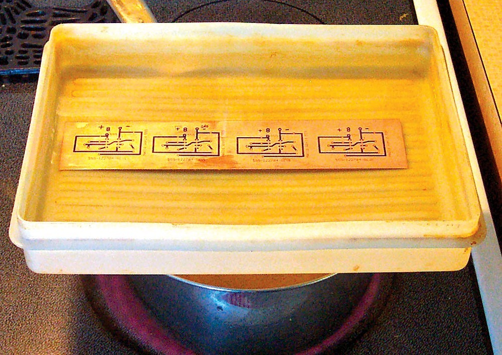
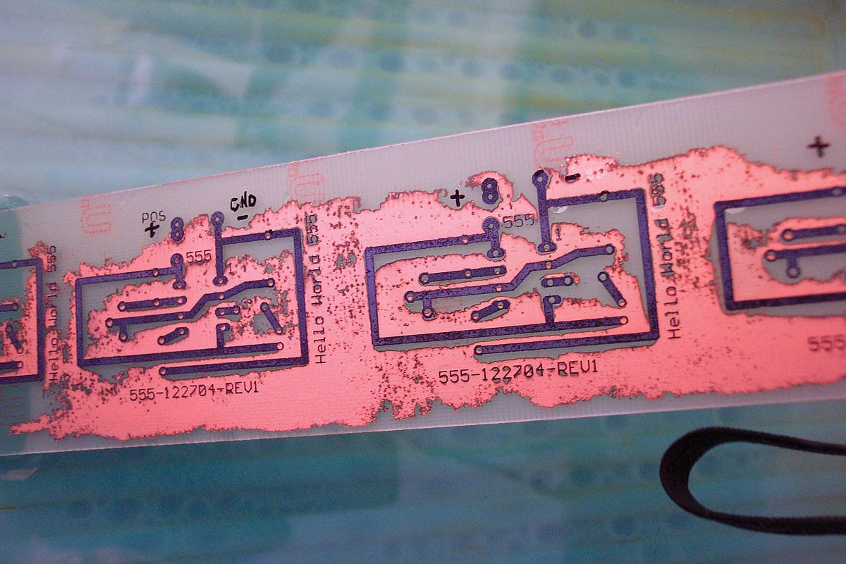
We’ll design our printed circuit on the computer, as a plain black-and-white image. Black represents where we want the board to have copper connections between our circuit’s components, while the white background corresponds to areas of plain, non-conducting fiberglass. Then we’ll print the design onto special transparency film and iron it onto the copper side of a blank PCB (which starts out with copper completely covering one side). We peel the film back off, and the printed design remains on the copper. Next, the magic happens: when we bathe the board in an etching solution, copper dissolves away in the blank areas of our design, leaving conductive “traces” behind where we had drawn the circuit’s connections. After this, we prepare the board for soldering, then finally go to town with the components.
Broken down step-by-step, the entire process can be summarized as follows:
-
Create the design.
-
Print or photocopy the design.
-
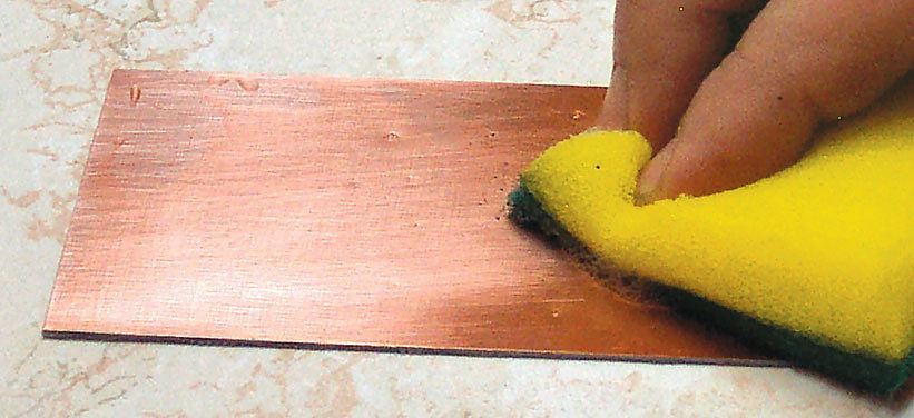
Prepare the PCB.
-
Transfer the design to the copper.
-
Check and correct the traces.
-
Etch the board.
-
Clean and drill the board.
-
Solder the components.
Materials
- Techniks Press-n-Peel PCB transfer film—(20 sheets for $30), techniks.com
- Ammonium persulfate crystals—(1Kg for $20), mgchemicals.com
- Black correction pen—(Lumocolor or fine-tip Sharpie)
- PCB copper board—(9 x 12 x 0.062-inch, 1 oz., single-sided, $12), techniks.com
- Circuit components
Tools
- Scouring pad—(do not use steel wool)
- Photocopier or laser printer
- Electric clothes iron
- Hard wooden board
- Large pot and plastic tray—for etching
- High-speed drill and bits
- Soldering materials
- Perf board and wire (optional)—for prototyping
NOTE: Techniks Press-n-Peel transfer film is a reasonable compromise between ease-of-use and cost. You could mask a board for etching with just a permanent marker, but this would take a long time, and it would be extremely difficult to make the lines sharp and accurate enough.


