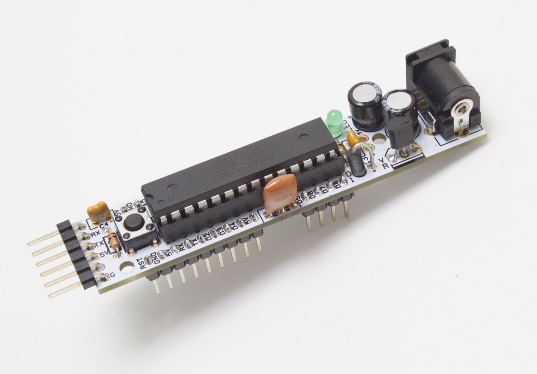
The Really Bare Bones Board

There are many tools for creating printed circuit boards, from the open source KiCAD to various online services. CadSoft’s EAGLE is a favorite in the open hardware community. Here you’ll learn the basics of PCB design in EAGLE, plus how to build the essential core of an ATmega microcontroller board.

The Really Bare Bones Board (RBBB) and its schematic were originally designed by Paul Badger of Modern Device. It’s pretty much the bare minimum needed for a useful Arduino-type development board. And once you build the schematic in EAGLE, it’s easy to incorporate in other designs.

NOTE: The part list, to right, gives the bill of materials for a single RBBB, but you don’t really need the components on-hand to follow along with the design tutorial below.

Jean-Claude Wippler of JeeLabs used the RBBB as a basis design for JeeNode, which has rearranged headers and an SPI radio port for wireless use.

Using EAGLE

EAGLE is a collection of programs, each serving one part of the design process. We’ll focus on Schematic Editor and Board Editor; other modules include Autorouter (trace layout AI), Parts Editor, CAM Processor (for creating machining-ready files), and a scripting interface for writing ULPs (User Language Programs).

Components are chosen from the parts library. Parts always have two representations: one for the schematic and one for the board. Most components come in different physical “packages,” and EAGLE’s libraries allow multiple packages to be associated with the same schematic symbol. To simplify things, I’ve created a custom RBBB library that includes only the parts in the packages you’ll need. Once you’re comfortable, SparkFun’s library is a good place to start expanding your horizons.

EAGLE DESIGN WORKFLOW

  1. Design and sourcing: Find parts, read datasheets, download or draw footprints.
  2. Schematic Layout: Connect parts electrically with signals.
  3. Electrical rule Check (ErC): Run an AI helper to identify schematic errors.
  4. Board Layout: Place parts on the board and draw the actual traces connecting them.
  5. Design rule Check (DrC): Run an AI helper to identify layout errors.
  6. Generate Gerber and drill files: Run CAM Processor to generate machining files.

PCB design takes several stages. This article guides you as far as drawing and validating the schematic, which should be enough to whet your appetite. The next piece in the series takes you through BLAH BLAH BLAH, and finally, part 3 wraps it up with BLAH BLAH BLAH.

Project Steps

1. Getting started.

Download EAGLE Light Edition from cadsoftusa.com. Also grab the RBBB library from moderndevice.com/downloads and place it in EAGLE’s /lbr directory.

EAGLE separates CAD drawings into color-coded functional layers coded functional layers. In Schematic Editor, part outlines are on the Symbols layer, labels on the Names/Values layers, and nets (aka signals) on the Net layer. You can show or hide the layers using the View menu.

TIP: Check the toolbar often to make sure you’re drawing into the right layer.

1.1. Open Schematic Editor and select File → New → Schematic. You’ll get a warning that “no forward/backward annotation will be performed.” Normally you’ll have both Schematic and Board Editor open at once so EAGLE can keep them synced; this message just says that there’s no board file open yet.

Figure 1.2

1.2. Choose the Add tool, grab the Frame part from the RBBB library, and place it on the canvas. It’s not essential, but it’s handy so you don’t have to keep resizing your window as the schematic grows.

2. The power circuit.

These 5 parts accept DC input power and output a clean 5V supply.

The centerpiece is the voltage regulator. The key specs for a regulator are output voltage, maximum output current, and dropout voltage, which is the minimum difference needed between input and output. The L4931 has a dropout of just 0.4V, so it can reliably output 5V given 6V (e.g. from 4 AA batteries). It provides current up to 250mA, which is plenty for most microcontroller applications.

The 2 electrolytic capacitors filter noise on the input supply, pick up slack when batteries fade, and handle momentary power demand spikes. The regulator’s datasheet recommends 2.2μF filter caps minimum; we’ll use 47μF. That should be stiff enough for even the noisiest battery-powered breadboard experi-
ments.

The power jack may seem big, but this is one of those human interface decisions that really matters — this jack easily accommodates a “wall wart” power supply. We’ll position it on the board where it can be snipped off if it’s unneeded, and provide a 2-pin auxiliary power header for optional wiring.

Almost any power diode will serve for short-circuit protection; this one is a common 4005 rated 1A, wired in parallel to prevent damage if power is accidentally connected backwards. Some designs opt for a series protection diode, but that would introduce a 0.7V drop we can’t afford if we want to run from 6V.

RULES OF THUMB

  • A dot indicates that intersecting signal lines are connected; lines that cross without a dot are just overlapping.
  • Stay on the grid. The most common mistakes come from parts not lining up, looking like they’re connected when they aren’t. Set it to 0.1 (100 mil) to start.
  • Each line (or net, or signal) has a unique name, and all signals with the same name are automatically connected, even if there’s not a line between them. This is handy if you have so many parts that drawing every line would make a pile of spaghetti.
  • Each part should have a visible name and a value. You’ll need to move the labels around to make them readable; use the Smash tool to separate labels from parts, then Move and Rotate to position them.
  • Drawing a schematic is about communicating a circuit assembly to someone else. Think about whether you’re providing everything they will need.

NOTE: Our diagrams may look different from your screen, at first. Remember to use Smash to separate the labels, then use Move so they’re readable.

Figure 2.1

2.1. Select the Add tool, choose RBBB → Regulator, and place the regulator somewhere in the upper left quadrant. Use the Add tool to place the 2 Electrolytic_Caps, plus GND and +5V supply signals (under RBBB → Supply), as shown.

Figure 2.2

2.2. Use the Net tool to connect the caps’ positive sides to the regulator’s input and output, and their negative sides to the regulator’s ground lead. Connect the regulator’s ground lead to GND, and its output to +5V.

2.3. Use the Value tool to assign each capacitor a value of 47μF.

Figure 2.4

2.4. Add RBBB → Power_Jack beside the regulator input. This jack is center-positive, which (outside of musical electronics) is pretty standard. Connect its center pin to the regulator input and its sleeve to ground. If you get a “Connect Net Segments?” dialog, select Yes.

Figure 2.5

2.5. Add the diode. It will appear horizontally. Use the Rotate tool to turn it cathode/negative side up. Then use the Net tool to connect it across the regulator input and ground.

Figure 2.6

2.6. Finally, drop in the 1×2 header (RBBB → 1x2_Pinhead) for the optional power input. Position it with Rotate, then connect one pin to power and one to ground.

3. The microcontroller and headers.

The headers connect to the microcontroller’s general-purpose inputs and outputs, and they provide “pans” for soldering wires or pins.

Figure 3.1

3.1. Add the microcontroller chip (RBBB → ATmega) somewhere in the middle of the schematic, and connect its 2 ground pins to the GND supply signal.

Figure 3.2

3.2. Place a 0.1μF capacitor near the ATmega’s power supply pin (7), and connect it to power, ground, and pin 7.

Figure 3.3

3.3. Place the resonator near clock pins 9 and 10, and connect its 3 pins as shown. Make sure the center pin goes to ground.

Figure 3.4

3.4. Create a signal line for all the other pins. Don’t forget analog reference (AREF) on the left. Use Net to connect a short signal to each pin, then use Label (right underneath) to label each one.

NOTE: EAGLE’s “group move” function does not work like most modern drawing software. If you need to move several parts at once, first use Zoom to zoom out, then choose Select and click-drag around the parts to be moved. Choose Move, left-click on the selected objects, Ctrl-right-click to get a menu, and choose “Move Group.”

Figure 3.5

3.5. You’ll see EAGLE gives a default label to each signal, something like N$2. Now use the Name tool to rename each signal to match its ATmega pin name. This is a bit tedious; if anyone knows a better way than manually, please let me know!

Figure 3.6

3.6. Add the 1×16, 1×9, and 1×4 header blocks and repeat the process of adding signals, adding labels, and changing names.

4. The serial header.

Figure 4

Our data interface is a 6-pin header connected to the ATmega’s serial port. The original Arduino had a USB port and an FTDI chip to translate from USB to TTL UART protocol. Moving this chip off the board and into the cable is an easy way to pare down the design. FTDI sells a cable with a 6-pin connector, or you can use a USB-BUB or FTDI Friend.

Place the 6-pin header and connect the RX (receive), TX (transmit), GND, +5V, and EXT_RESET pins.

5. Amenities.

Many designs skimp on human factors, with tiny buttons, inconvenient part arrangements, and indecipherable labels. Don’t do this. Our design includes a generously sized reset button and an LED “pilot light” to clearly show when the board is powered.

Figure 5.1

5.1. Position the switch, the 10K resistor, and the remaining 0.1μF capacitor as shown. Connect one side of the switch to ground.

The switch is normally open, but pulls RESET low when pressed. The 10K resistor is connected between RESET and +5V so that the pin is not “floating” (which can cause erratic behavior) when the switch is open. During programming, the host computer pulls EXT_RESET low to reset the chip before the bootloader starts loading code. The small capacitor keeps the timing of this pulse within the limits expected by the system.

Figure 5.2

5.2. Finally, add an LED in series with a 1K current-limiting resistor.

6. Check the circuit.

Run the Electrical Rule Check by selecting ERC from the Tools menu. You’ll get a list of errors and warnings; click on them to make any needed fixes. A common mistake is for lines to be very close without actually connecting.

Going further

Once you’ve passed the ERC, select File → Switch To Board and you’ll be asked if you want to create a new board from the current schematic using the Layout Editor. Yes! From now on you’ll want to have both schematic and board windows open whenever you’re working. EAGLE will keep the two in sync, but only if they’re both open.

Figure 7.1
Figure 7.1

Now you’ll route the actual copper traces on your board. EAGLE can do this automatically, but it’s a good idea to try your hand at manual routing, just to understand it. First you’ll draw the boundary of the board and set the spacing grid. Then you’ll lay out the power circuit, place the components, and route the GPIO traces, connecting top to bottom traces where necessary (Figure 7.1). Finally, you’ll add a ground plane to the bottom of the board (Figure 7.2).

Figure 7.1
Figure 7.1

After routing, the only steps left are to create the silk-screen layer and the Gerber and drill files to be sent to the PCB house for manufacturing. Click here to go on to part 2, with step-by-step instructions for laying out your board, and part 3, for producing silk-screen, Gerber and drill files.