Making your own printed circuit boards (PCBs) is so easy now. The biggest change is in the resist coating on the boards. Now it is less sensitive to ambient light. You do not need a safelight or a closed room to work with these new boards. You do have to be careful with direct light from any source for more than a minute or so. You do not need a special bulb to expose them. Sunlight or a fluorescent light works best.
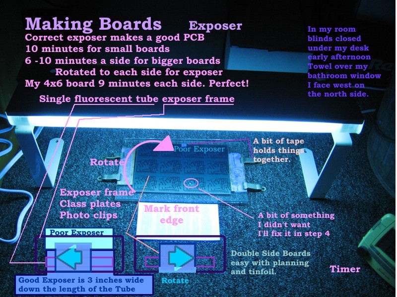
Plan your space. I closed my bedroom blinds early in the afternoon and placed the exposer frame under my desk. I put a towel over my bathroom window where I have the development tray filled and set up. That’s it.
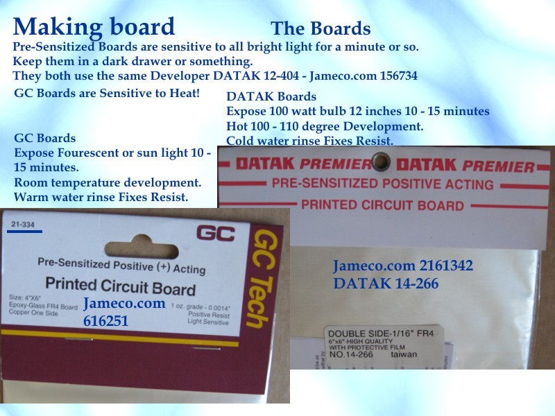
The DATAK Boards use the same developer. They require a Hot 100 – 110 degree water development and a Cold water rinse to fix the resist. They can be exposed with standard 100 watt bulb at 12 inches for about 10 – 15 minutes.
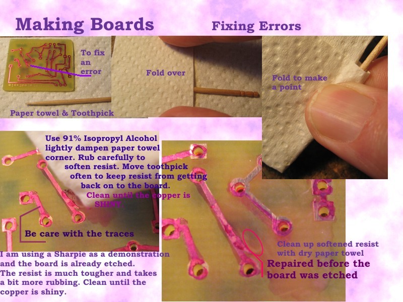
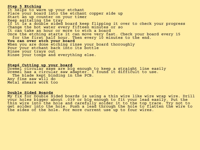
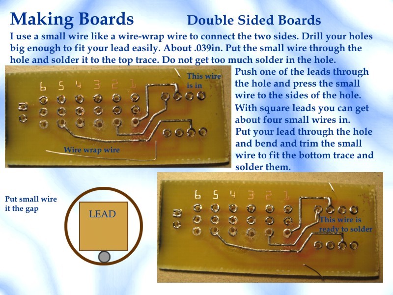
One thing that is important is that the resist is now sensitive to heat. Any heat. Storing a board in its package under direct sunlight will kill your board. Keep them in a cool dark place. Heat is a good thing too. When you are done developing your board you just rinse the board under warm water and that fixes the resist. Caution here. Once the resist is fixed it is not sensitive to the developer or the light anymore. At this point 91% isopropyl alcohol cleans off the resist and you can fix errors or do modifications all in normal light.
One downside to these single fluorescent tube exposer frames is that the area of good light is just three inches wide down the length of the tube. A 4×6 board set at the front of the exposer frame will have its back one inch poorly exposed. You must rotate your board. For big boards just move them three inches each step through the exposer. Expose for about 6-8 minutes per step. You can get larger multi-tube exposer frames and special exposer lights.
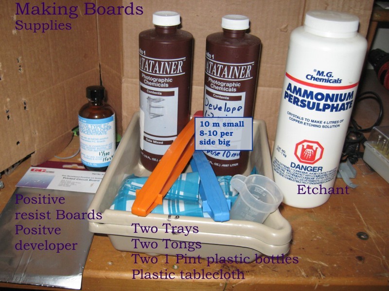
Jameco has everything to make a PCB at home: positive resist boards, positive developer, etchant, trays and an exposer frame. Look under Electronic Design → Prototyping Systems. Pre-sensitized boards are available in many standard sizes. The More Products category has PCB kits and stuff. I have a single 17" fluorescent tube exposer frame. Mine is about 5 ½" high. I got it at Fry’s in Burbank, Ca. I also got my Ammonium Persulphate etchant at Fry’s. Read the instructions that come with the boards. A good exposure makes a good PCB.
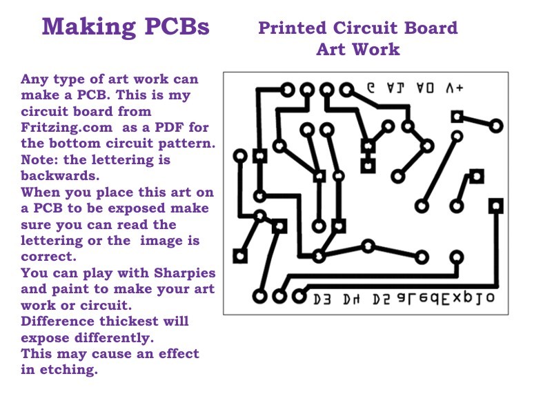
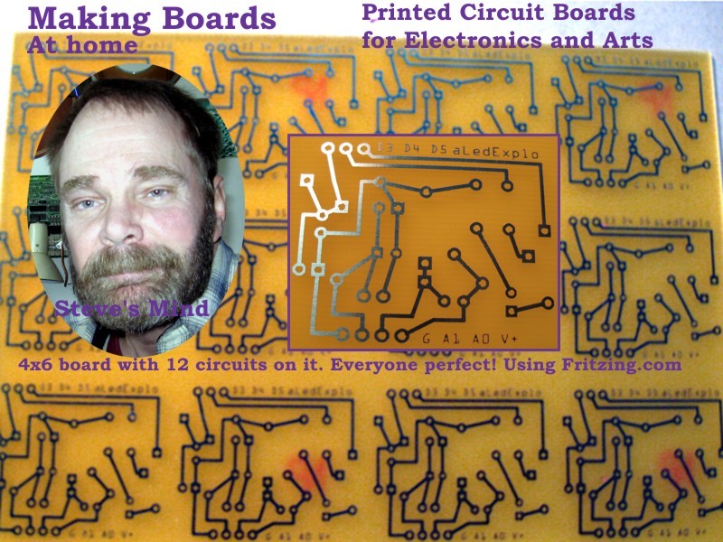
I use Fritzing.org to design my boards. Fritzing’s software lets you export your design to a PDF file. Print the PDF file at 100% on clear transparency sheets. For laser printers print on the smooth side of the transparency sheet. Cut out the circuit on the board’s outline.
To work with Fritzing you need electronics knowledge and desktop publishing experience. An example is the object label used in all views. Right-click the object and select Show Label. Select the object and left-click the label and drag it. Right-click the label, select Edit, Size, Rotation and Display Details.
You must get the breadboard and the schematic perfect before you can get a good PCB. No “birdcage wires” (Fritzing calls them “rat’s nest” wires) anywhere. Test all circuit paths by clicking on a node. Then in the PCB remove any rat’s nest wires, rotate and move the parts and delete and make new circuit paths. You make big changes in the breadboard view first, then the schematic view if you need it and then the PCB view.
In the PCB view deleting a trace is the same as deleting a wire in the breadboard and the schematic views. Complete your changes in the PCB and check for rat’s nest wires in the other views. Make wires out of the correct connections and delete the rest. The default PCB is double-sided. Auto-routing is automatic in the other views as you add parts and wires. Start moving, orienting and wiring each part on your PCB as you add them.
To make multiple circuits on one PCB, save your project as somethingA10. In PCB view click the PCB and in the Parts menu set Sticky to unchecked. Click and drag the PCB away from your circuit. Set your PCB to the size that you need. 4×6 is width 101.6mm and height 152.4mm. Position your circuit to the left of the PCB and close to where the duplicate will go.
Drag a selection box around your circuit. Let go. In the edit menu select Duplicate (Ctrl-D). Wait for the duplicate circuit to show up. Do not click it. Use the arrow keys to move your duplicate onto your PCB. Repeat this for each copy. The breadboard and schematic views will be a mess. Line things up nicely. Save your project. Make an editable PDF. Wait for it. Done.
I do not put Sticky back on. Watch out for Duplicate errors. All of the part labels have copy numbers in them. Do not touch the breadboard or the schematic. To fix errors delete the bad circuit and make a new duplicate circuit. The more parts in the circuit the longer it will take to make a duplicate.